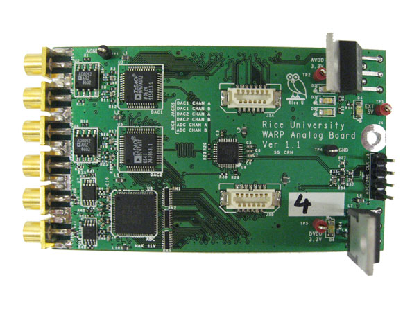
WARP Analog Board
The WARP Analog Board is a debug daughtercard that has 4 channels of Digital-to-Analog conversion and 2 channels of Analog-to-Digital conversion. The digitial-to-analog conversion is done by two dual-port, 14-bit, 125MSPS DACs (AD9767). The analog-to-digital conversion uses a dual-port, 14-bit, 65MSPS ADC (AD9248). The analog interface is handled by MCX jacks with a maximum output voltage swing of 2Vp-p. All necessary clocks are generated locally on the board as well.
Additionally, we provide a hardware bridge core to ease the use of this daughtercard when used in conjunction with the WARP FPGA board. The core implements all necessary details, with input and output ports visible in Xilinx Platform Studio for the user to connect to.
An interface for a subsequent card is also provided, if needed, for use of further I/O.
WARP Analog Board Design Files
The analog board design files are available in the WARP repository.
Users Guide
The users guide for revision 1.1 of the board is available here.
