| Version 1 (modified by murphpo, 18 years ago) (diff) |
|---|
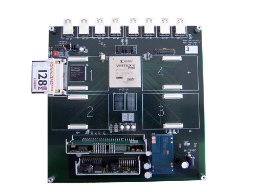
WARP FPGA Board
The WARP hardware must provide substantial processing resources to meet the computational needs of wireless systems operating at 100s of Mb/sec. Wireless algorithms require a large number of DSP-centric computations, yet DSPs and other similarly structured processors do not provide nearly enough processing power. We chose FPGAs as the WARP processor. Large FPGAs provide tremendous processing resources composed largely of parallel, programmable logic blocks which can be interconnected to form complex functional units. FPGAs are also extremely well suited for DSP-intensive operations, especially in applications where algorithms can be parallelized. For example, the front-end processing for many wireless applications requires high-throughput operations like filters and correlators replicated for each wireless interface. Implementations of these operations can exploit parallel structures in hardware to improve performance. Further, each instance of a functional unit operates in parallel with all others. Such multi-level parallelism is a key way FPGAs provide performance far beyond the capabilities of even the most powerful DSP.
The main board in the platform is the WARP FPGA board. At the heart of this design will be a Xilinx Virtex-4 FPGA, the latest and most powerful available. These FPGAs are very well suited for the kinds of DSP-intensive operations which the various applications for WARP will require. For example, the Virtex-4 provides dedicated DSP slices, hardware blocks designed specifically for high speed multiply-accumulate and other DSP operations. These slices are a feature not available in the FPGA used by the TAP platform and will play a major role in implementing computationally intensive wireless algorithms on WARP. Virtex-4 FPGAs also provide flexible and fast interconnect options for interfacing peripherals and creating multi-processor systems, two primary requirements of the platform design. Some versions of Virtex-4 also include embedded PowerPC processor cores, providing an ideal resource for implementing higher layer algorithms better suited for general purpose processors than programmable logic.
Daughtercard Slots
While the FPGA itself provides substantial processing power, its connections to other devices and boards will enable the variety of applications targeted by WARP. The WARP FPGA board will provide four daughtercard slots, each wired to a large number of dedicated FPGA I/O pins. These slots will house peripheral cards (two example daughtercard designs are described below). The slots will be flexible enough to support a wide variety of future peripheral designs, including multimedia interfaces and specialized auxiliary processors. The four slots will be functionally identical, allowing users to mount the combination of peripheral cards that best suits their application. The slot interface will be backwards compatible with the TAP daughtercard specification. This interface will be documented in the WARP repository, allowing WARP users to design custom daughtercards.
Board-to-Board Links
A major challenge in designing an FPGA-based platform for computationally intensive applications is connecting multiple FPGAs together to accommodate algorithms which are too complex to fit on a single chip. A common approach is to design hardware with multiple FPGAs on a single board. Such designs have the benefit of proximity of computational resources, guaranteeing low-latency communication between processors. Two major drawbacks to this approach, however, are the added hardware design complexity and potential for wasted resources in applications which require fewer FPGAs than those mounted on a single board. We expect such applications to be common among WARP users, especially in the early stages of algorithmic implementation. Thus, the WARP FPGA board will be built around a single large FPGA.
This presents the challenge of connecting multiple FPGAs together when the need arises. We address this scalability requirement by utilizing the multi-gigabit transceivers built into Virtex-4 FPGAs. Each MGT provides a full duplex 3+ Gb/sec connection between two FPGAs; multiple MGTs can be used in parallel to provide even more throughput between two boards. Eight MGTs will be routed to off-board connectors on each WARP FPGA board, providing substantial (24 Gb/s) inter-FPGA communications capabilities. A frequently cited drawback to MGTs is their relatively high latency. These delays are imposed by the transceivers in order to combat reference clock frequency offsets. The WARP hardware will bypass this limitation by providing flexible clock resources which can be shared among multiple FPGA boards. Transceivers which share a reference clock can communicate with significantly lower latencies, usually on the order of a few cycles. Independent clocking will also be supported for situations where MGTs are used to interface with non-WARP hardware.
