| Version 11 (modified by murphpo, 12 years ago) (diff) |
|---|
WARP v3 Getting Started Exercises
Developing custom applications on WARP requires using design tools from Xilinx. These tools are sophisticated (i.e. they're complicated) and can be daunting to a new user. We've created some simple exercises that introduce the core tools most WARP users will use.
Basic Design Structure
All WARP reference designs are built using the Xilinx Embedded Development Kit (EDK). The EDK enables construction of designs with both a processor, for running custom software, and custom hardware cores for real-time processing and connecting to off-chip hardware.
The EDK includes two primary tools:
- Xilinx Platform Studio (XPS): integrates the hardware cores for a design, including the MicroBlaze processor, memory, peripherals and interfaces for off-chip hardware
- Xilinx Software Development Kit (SDK): a full suite of software compilation and debugging tools for the MicroBlaze processor
The basic structure of WARP reference designs is illustrated below.
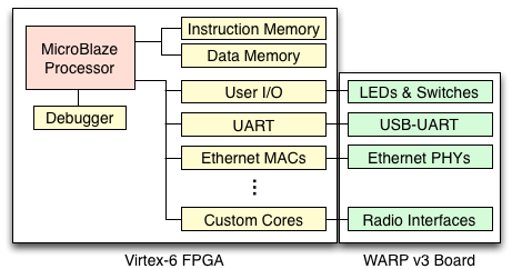
The MicroBlaze processor and connected cores are all implemented in the FPGA fabric using XPS. The output of the XPS flow is a "bitstream" with the fully synthesized and implemented hardware design. This bitstream integrates the MicroBlaze, the standard peripheral cores, your custom cores, I/O assignments, clock configurations and timing constraints. However the MicroBlaze instruction and data memories are blank in this bitstream.
The XPS-generated bitstream (and its associated hardware specification) is the starting point for an SDK project. The SDK compiles custom code for the MicroBlaze, along with drivers for the various cores included in the XPS hardware design. The output of this process is an "elf" file, the software binary ready for execution by the MicroBlaze. The elf binary is combined with the XPS-generated bitstream to program the FPGA with the final hardware+software design.
Exercises
SDK Intro:? This is the classic "hello world" project for WARP v3 using the Xilinx SDK. We provide an already-built bitstream with a MicroBlaze and some basic peripheral cores. This exercise uses the SDK to write some simple C code, compile it for the template hardware project and download the harware+software design to the WARP v3 board. At the end of this exercise you should be comfortable with the basic software design flow using the SDK.
XPS Intro:? This exercise introduces
- Exercises/SysGenExport? - In this exercise, users will instead control the LEDs on the board with an FPGA design constructed in Xilinx System Generator. The process this exercise takes you through mirrors the steps that would occur if this peripheral core were a new physical layer.
In addition to being well-suited for real-time physical layer implementations, WARP also allows physical layers to be rapidly prototyped through the WARPLab design flow. WARPLab allows physical layers to be designed directly in Matlab and prototyped through actual over-the-channel transmissions while processing occurs offline on your computer.
I Want to Study the Higher Networking Layers
One of the most common networking applications for WARP is the study of novel medium access control (MAC) protocols. Typically, MACs are implemented as software written in C and run on a MicroBlaze processor core in the FPGA. As such, the best example to start with is:
- Exercises/HelloWorld? - The Hello World exercise is what we recommend all new users of WARP start with. By the end of it, users will use C-code to control LEDs on the board as well as print messages over UART.
After that, it is best to jump to the OFDM Reference Design and set up a link using the CSMA MAC code included in the design. This serves as a good example on how to write custom MAC software for WARP.