WARP Clock Board
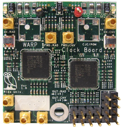
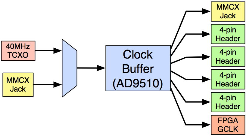
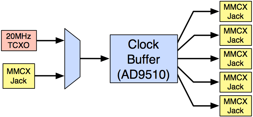
The WARP Clock Board is designed to provide the clock signals for all parts of a wireless design. It contains two sections. The first provides reference clocks for WARP radio boards. The second provides clocks for FPGA logic and analog converters. Both sections have the option of accepting their clock input fron an on-board temperature compensated crystal oscillator (TCXO) or via an off-board connector. The latter option allows multiple WARP nodes to share common clocks for beamforming or multi-FPGA applicaitons.
Sampling & Logic Clocks
Please see Connectors for a guide to the connectors in this section.
Radio Reference Clocks
Please see Connectors for a guide to the connectors in this section.


