FMC-BB-4DA User Guide: FMC LPC Interface
The FMC-BB-4DA module is designed (with a few deviations, explained below) to the VITA 57.1 FMC specification. This module has been tested in the FMC slot on WARP v3 kits. The details below will help determine compatibility with third-party FMC carriers.
Power
The FMC-BB-4DA module draws all its power from the FMC carrier. The required power supplies are:
| FMC Net | Supported Voltages | Use |
|---|---|---|
| VADJ | 1.8v - 2.5v (see notes) | AD9116 digital interfaces |
| 3P3V | 3.3v | AD9116 analog power supplies |
| 3P3VAUX | 3.3v | EEPROM power supply |
Other power connections on the FMC-RF-2X245 module:
- 12P0V is not used
- 3P3VAUX is only used for the EEPROM
- VIO_B_M2C is tied to VADJ (on HPC carriers this will power VCCO for Bank B with VADJ, even though this module does not use any HB I/O)
- VREF_A_M2C/VREF_B_M2C are unconnected
- PG_M2C is tied to PG_C2M
VADJ note: the FMC VADJ net is tied to the digital interface power supplies of multiple circuits on the FMC-BB-4DA module. These interfaces are all specified over the range 1.8-2.5v. However, we have only tested this module on the WARP v3 kit, which ties VADJ to 2.5v.
FPGA I/O
The FMC-BB-4DA module uses I/O from the LA bank and will function with either LPC or HPC FMC carriers. All I/O are used as signal ended signals.
Four I/O in the HA bank are tied to ground, for routing improvements on the PCB. All I/O in the HB bank are unconnected.
The module does not generate any clock signals. Occupied CC signals in the LA bank are used for general I/O.
MGTs
The FMC-BB-4DA leaves all FMC MGT interfaces (the DPx and GBTCLKx signals) unconnected.
Misc I/O
JTAG: The FMC JTAG signals are not used by circuits on the FMC-BB-4DA module. The module ties TDI to TDO to complete the carrier JTAG chain. TCK and TMS are not connected on the module.
EEPROM: A Microchip 24AA128 I2C 128Kb EEPROM is connected to the FMC I2C signals (SCL, SDA). Refer to the EEPROM page of this guide for details on the default EEPROM contents.
Mechanical
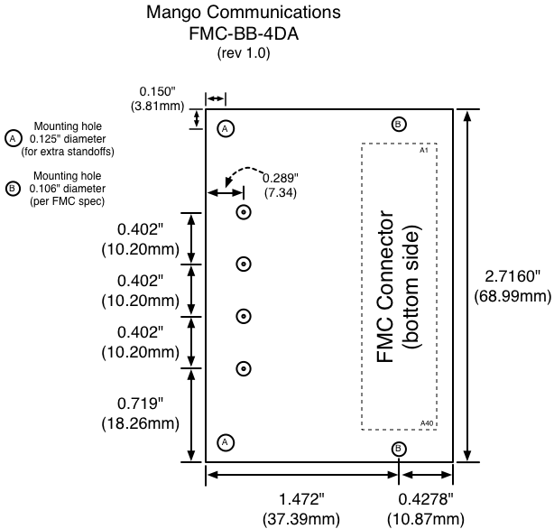
FMC-BB-4DA modules are built with either the MC-LPC-10 or MC-HPC-10 connector options (lead-free, LPC/HPC, 10mm stacking height). The module includes two mounting holes on either side of the FMC connector at the locations specified in the FMC standard. The module ships with 10mm standoffs pre-installed and mating screws for securing the module on the FMC carrier.
The FMC-BB-4DA module dimensions are not strictly compliant with the mechanical specifications for FMC modules in VITA 57.1.
The module dimensions are compliant in the region around the FMC connector. This is sufficient for mechanical compatibility with many FPGA carriers (including WARP v3) which orient their FMC slots with modules extending away from the carrier board.
The FMC-BB-4DA module deviates from the standard at the other end of the board. The FMC-BB-4DA module is a rectangular PCB, while the FMC standard specifies a more complex shape which narrows at the connector end. This module is also shorter than a standard module.
The deviations from the FMC outline specifications are not an issue when using this module on WARP v3 kits, nor on many other FMC-equipped FPGA development platforms we have seen. However the drawing below and electrical/IO/clocking details above should be carefully considered before using the FMC-RF-2X245 module on a third-party FMC carrier.

FMC-BB-4DA Mechanical Drawing (PDF version)
Pinout
A pinout file is available in the repository: Mango_FMC-BB-4DA_WARPv3_Pinout.ucf. This text file provides the mapping of FMC-BB-4DA signals to FPGA pins on the WARP v3 kit, using the standard Xilinx UCF syntax. Each pin assignment also includes a comment with the FMC net name, using the FMC standard nomenclature (LA09_N, LA00_CC_P, etc.)