| Version 1 (modified by murphpo, 11 years ago) (diff) |
|---|
WORK IN PROGRESS - DON'T TRUST THIS DOCUMENTATION JUST YET...
FMC-RF-2X245 User Guide: RF Interface Clocking
The FMC-RF-2X245 module RF interfaces require two clocks.
The first, the RF reference clock, drives the reference clock input of the MAX2829 transceivers. The transceiver use this clock to generate their RF carrier signals. The two transceivers always share the RF reference clock source, ensuring synchronous RF carriers across interfaces.
The second clock, the sampling clock, drives the AD9963 (the combined dual ADC/DAC). The host FPGA must also have access to this clock.
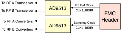
By default the FMC-RF-2X245 module sources these clock signals from the FMC header.
FMC Clocking
When built for FMC clocking, the FMC-RF-2X245 module requires the FMC host to drive appropriate clocks on two dedicated FMC clock pin pairs. Both clock signals must be very low phase noise to preserve the performance of the RF interfaces. The two clock signals can be synchronous, but the FMC-RF-2X245 module does not require this.
The WARP v3 board connects these FMC pins to the clocks used by its on-board RF interfaces. Thus FMC-RF-2X245 modules used on WARP v3 kits are configured at build-time for FMC clocking.
| Clock | FMC Signal | FMC Pins | Frequency |
|---|---|---|---|
| Sampling | CLK2_BIDIR | K4/K5 | Depends on AD9963 config |
| RF reference | CLK3_BIDIR | J2/J3 | [20, 40, 80] MHz |
Clock Buffer Configuration
The FMC-RF-2X245 module uses two AD9513 clock buffers to distribute the sampling and RF reference clocks. The AD9513 buffers are configured by a DIP switch on the FMC-RF-2X245 module (SW1). The configuration options and corresponding switch settings are explained below.
The DIP switch has six separate switches, labeled 1-6 on the component itself. Each switch is On or Off, where the On position is labeled on the switch. See the figure below for details.

The DIP switch settings should only be changed when the module is unpowered.
Sampling Clock Buffer
The sampling clock buffer has three outputs:
- OUT0: connected to converters (AD9963) for RF A
- OUT1: connected to converters (AD9963) for RF B
- OUT2: connected to FMC CLK0_M2C (LVDS signal driven to FMC pins H4/H5)
The divider for OUT0/OUT1 can be configured to 1, 2 or 4 via the DIP switch:
| Divider | SW[x] | SW[y] |
|---|---|---|
| 1 | x | x |
| 2 | x | x |
| 4 | x | x |
The output to the FMC header (OUT2) can be en/disabled via the DIP switch:
| OUT2 | SW[x] |
|---|---|
| Off | x |
| On | x |
The output to the FMC header (OUT2) should only be enabled when the FMC-RF-2X245 module is built for on-board clocking. When using the FMC-RF-2X245 module on a WARP v3 kit the FPGA receives the sampling clock directly and does not require another copy be driven to the FMC slot.
RF Reference Clock Buffer
The sampling clock buffer uses a single output to drive both RF interfaces. The only configuration option is the divider applied by the AD9513. The same divider value is always used for both RF interface reference clocks.
The divider should be chosen to comply with the MAX2829 reference clock frequency requirements. Typically the MAX2829 requires a 20MHz or 40MHz reference clock input.
| Divider | SW[1] | SW[2] |
|---|---|---|
| 1 | x | x |
| 2 | x | x |
| 4 | x | x |