WARP FPGA Board MGTs
The Virtex-4 FPGA is equipped with 10 pairs of differential multi-gigabit transceivers. Each MGT is a full-duplex transceiver supporting serial data rates up to 6.5 Gbps. The WARP FPGA board includes 8 MGT interfaces: 4 HSSDC2, 2 SATA and 2 SFP.
The MGTs on the Virtex-4 FPGA are internally organized in two columns. Each column has two clock inputs and all the MGTs in the column can use either of those clocks. Our design maximizes the functionality by allowing the user to select the clock frequency that is input to the columns.
All the MGT connectors are located on the north side of the FPGA Board; both on the top and bottom.
MGT Interfaces
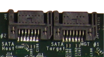
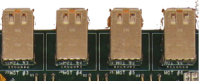
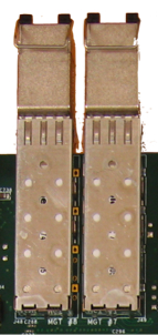
There are three types of MGT connectors on the board. Two Small form-factor Pluggable (SFP) are connected to one column in the FPGA. The HSSDC2 and SATA interfaces are connected to the other column.
 |  | 
|
| SATA Interfaces | HSSDC2 Interfaces | SFP Interfaces |
The MGT interfaces are labeled "MGT 1" to "MGT 8" on the WARP FPGA board. The table below shows the mapping of each interface to the corresponding MGT in the FPGA.
| MGT # | Type | Connector | MGT Tile | Column | LOC Constraint | TXP | TXN | RXP | RXN | Ideal Clocks |
| 1 | SATA Target | J47 | 112B | 1 | GT11_X1Y4 | P1 | R1 | U1 | V1 | MGTCLK_110 or MGTCLK_113 |
| 2 | SATA Host | J46 | 112A | 1 | GT11_X1Y5 | M1 | N1 | J1 | K1 | MGTCLK_110 or MGTCLK_113 |
| 3 | HSSDC2 | J3 | 113B | 1 | GT11_X1Y6 | A4 | A3 | C1 | D1 | MGTCLK_110 or MGTCLK_113 |
| 4 | HSSDC2 | J4 | 113A | 1 | GT11_X1Y7 | A6 | A5 | A9 | A8 | MGTCLK_110 or MGTCLK_113 |
| 5 | HSSDC2 | J5 | 114B | 1 | GT11_X1Y8 | A14 | A13 | A11 | A10 | MGTCLK_110 or MGTCLK_113 |
| 6 | HSSDC2 | J6 | 114A | 1 | GT11_X1Y9 | A16 | A15 | A19 | A18 | MGTCLK_110 or MGTCLK_113 |
| 7 | SFP #1 | J49 | 102A | 0 | GT11_X0Y7 | A34 | A35 | A31 | A32 | MGTCLK_102 or MGTCLK_105 |
| 8 | SFP #2 | J48 | 102B | 0 | GT11_X0Y6 | A36 | A37 | C39 | D39 | MGTCLK_102 or MGTCLK_105 |
MGT Clocking
The WARP FPGA Board provides very flexible MGT clocking. The Virtex-4 FPGA organizes the MGTs into two columns. Each column provides two clock inputs. An MGT can use either clock driven into its column.
The FPGA Board provides five MGT clock sources- four oscillators and one off-board interface. Two oscillators are installed by default; the remaining oscillator footprints can be populated as needed to support custom applications.
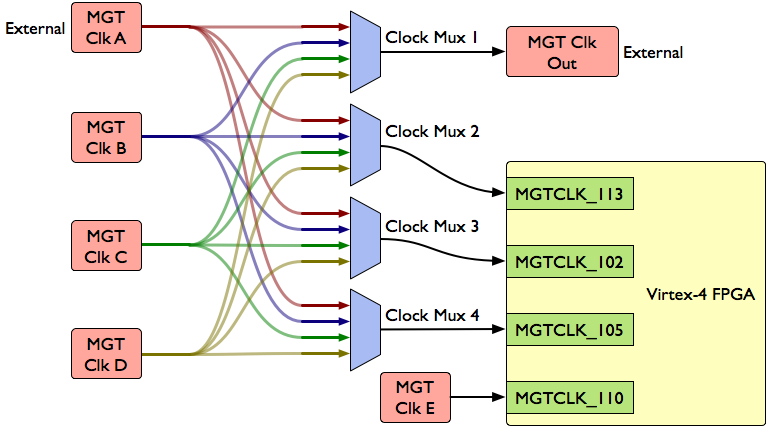
One oscillator is connected directly to an FPGA MGT clock input. The remaining clock sources (four oscillators and the off-board interface) are connected to the FPGA through a flexible multiplexer network. This network allows the user to assign any of the four clock sources to any of the three FPGA MGT clock inputs. It also provides an off-board clock output which can be connected to another FPGA board, allowing multiple FPGA boards to share an MGT reference clock.
The image and tables below provide details for the WARP FPGA Board's MGT clocking system.
MGT Clock Sources
| Clock Source | Component | Mux Input | Source |
| MGT Clk A | J14 or J11/J18 | 0 | Off Board Connectors |
| MGT Clk B | Y2 | 1 | Oscillator (Not Installed) |
| MGT Clk C | Y3 | 2 | 250MHz Oscillator |
| MGT Clk D | Y4 | 3 | Oscillator (Not Installed) |
| MGT Clk E | Y8 | - | 300MHz Oscillator |
FPGA MGT Clock Inputs
| Clock Input | Tile | Column | GT11CLK LOC | P Pin | N Pin | Source |
| MGTCLK_102 | 102 | 0 | GT11CLK_X0Y3 | F39 | G39 | Mux 3 |
| MGTCLK_105 | 105 | 0 | GT11CLK_X0Y1 | AW34 | AW33 | Mux 4 |
| MGTCLK_110 | 110 | 1 | GT11CLK_X1Y1 | AW6 | AW7 | MGT Clk E (Y8) |
| MGTCLK_113 | 113 | 1 | GT11CLK_X1Y3 | F1 | G1 | Mux 2 |
MGT Clock Mux Network
There are four clock multiplexers on the board, each with four inputs. All four muxes have the same four inputs, labeled MGT Clk A - E. The output of Mux1 drives the off-board clock output. The other three muxes each drive an FPGA MGT clock input.
Each mux is configured by 2 bits, selected by 2 positions on a DIP switch. Two 4-position DIP switches (SW11 and SW10) provide the 8 bits of configuration (2 bits per mux).
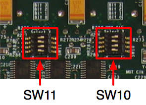
Multiplexer output select switches
The assignment of DIP switches to muxes is shown in the figure below. The highlighted switches identify the positions responsible for a given mux. The two DIP switches are drawn as viewed on the bottom of the WARP FPGA Board.
 |  |  | 
|
| Mux 1 | Mux 2 | Mux 3 | Mux 4 |
Mux Configuration Switch Assignments
Each 2-switch pair selects one of four clock sources. The mapping of clock source to switch values is illustrated below.
 |  |  | 
|
| Clk A | Clk B | Clk C | Clk D |
Mux Configuration Source Selection
Off-Board MGT Clock Connections
The FPGA Board provides input and output interfaces for inter-board MGT clock connections. Each interface is composed of three connectors- 2 MMCX jacks, (for dual-coax cables) and a 4-pin 0.1" male header (for twisted pair cables). Only one cable type (either dual-coax or twisted pair) should be used per interface. The image below shows the interfaces on the FPGA Board.
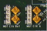
External MGT clock input and output
Connectors & Cables
Four MGTs are wired to Infiniband-keyed HSSDC2 jacks. You must use an Infiniband-keyed 100Ω HSDDC2-HSDDC2 cable to connect two FPGA boards together. One such cable is made by Molex (Molex HSDDC2 Cables).
The two SFP connectors require an additional module. One common SFP module is a Gigabit Ethernet interface. We have successfully tested two Gigabit Ethernet modules: Molex part 74741-0005 (available from Digikey) and Add-On Computer part GLC-T-AO (details). Other modules which adhere to the SFP specification should work as well.
Designing with MGTs
Xilinx provides extensive documentation for the Virtex-4 MGTs in the Virtex-4 RocketIO Multi-Gigabit Transceiver User Guide).
We have created an example design that uses the SFP Ethernet in a cabled loopback setup.
Every user design for the Virtex-4 must instantiate the MGTs or their performance will degrade over time (Xilinx app notes here and here). Xilinx provides the MGT Protector (datasheet here) that keeps the MGT tiles in a powered on state during the operation of the FPGA. An example of usage can been seen in the OFDM Reference Design v14.1.


