WARP v3 User Guide: Clocking
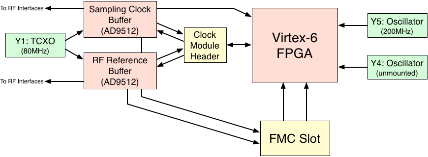
Clocking in WARP v3 is very flexible. An overview of clocking resources is shown in the figure below. Each subsystem is explained in detail below.

FPGA Oscillators
There are two oscillators connected directly to the FPGA: Y4 and Y5.
Y5 is a 200MHz LVDS oscillator (typically an SiTime SiT9102AC). The clock outputs are tied to a differential global clock input on the FPGA. The LVDS termination resistor is not included on the WARP v3 board. You must use the FPGA's internal LVDS termination via the DIFF_TERM constraint. The UCF snippet below includes this.
NET "osc200MHz_p" LOC = "A10" | IOSTANDARD = "LVDS_25" | DIFF_TERM = "TRUE";
NET "osc200MHz_n" LOC = "B10" | IOSTANDARD = "LVDS_25" | DIFF_TERM = "TRUE";
Y4 is unmounted by default and can be populated by the end-user if needed. The Y4 footprint will accommodate standard 2.5v oscillators in 5x3.2mm or 3.2x2.5mm packages.
#Oscillator Y4 is un-mounted by default
NET "osc_Y4" LOC = "H28" | IOSTANDARD = "LVCMOS25";
FMC Clocks
There are multiple clock connections to and from the FMC slot. For details see the FMC page.
RF Interface Clocking
The RF interface clocking design is centered on two AD9512 2-to-5 clock buffers. One AD9512 manages the sampling clock, the second manages the RF reference clock. Refer to the AD9512 datasheet for details on the operation of the clock buffers.
Both AD9512 buffers have SPI interfaces for configuration at run time. The SPI interfaces are connected to dedicated FPGA pins. The FPGA must implement an SPI master to configure the clock buffers. We have written the w3_clock_controller core to manage both clock buffers from user code in processor-based designs in the FPGA.
The FPGA connections for the clock buffer configuration interfaces are listed in the UCF snippet below.
#RF Ref Clock Buffer Config
NET "RF_CLK_SPI_SCLK" LOC = "V25" | IOSTANDARD = "LVCMOS25";
NET "RF_CLK_SPI_SDIO" LOC = "W25" | IOSTANDARD = "LVCMOS25";
NET "RF_CLK_SPI_CSB" LOC = "W27" | IOSTANDARD = "LVCMOS25";
NET "RF_CLK_SPI_SDO" LOC = "Y27" | IOSTANDARD = "LVCMOS25";
NET "RF_CLK_FUNC" LOC = "L26" | IOSTANDARD = "LVCMOS25"; #

#Samp Clock Buffer Config
NET "SAMP_CLK_SPI_SCLK" LOC = "W32" | IOSTANDARD = "LVCMOS25";
NET "SAMP_CLK_SPI_SDIO" LOC = "Y29" | IOSTANDARD = "LVCMOS25";
NET "SAMP_CLK_SPI_CSB" LOC = "W31" | IOSTANDARD = "LVCMOS25";
NET "SAMP_CLK_SPI_SDO" LOC = "Y28" | IOSTANDARD = "LVCMOS25";
NET "SAMP_CLK_FUNC" LOC = "R33" | IOSTANDARD = "LVCMOS25";
Sampling Clock
The connections for the sampling clock buffer (U46, AD9512) are summarized in the table below.
AD9512 Port Connection Logic CLKIN1 80MHz TCXO - CLKIN2 Clock module header (pins 23/25) - CLKOUT0 RFB ADC/DAC LVPECL CLKOUT1 Clock module header (pins 29/31) LVPECL CLKOUT2 RFA ADC/DAC LVPECL CLKOUT3 FPGA U23/V23 LVDS CLKOUT4 FMC CLK2 BIDIR LVDS
Notes:
- All outputs on the AD9512 are enabled by default. You should disable unused outputs in your design. Refer to the reference projects for sample code.
- CLKOUT3 drives an LVDS clock to the FPGA. The LVDS termination resistor is not included on the WARP v3 board and must be implemented in the FPGA. This clock is connected to an MRCC (multi-region clock capable) pin in column 2 of the FPGA and is capable of driving any clock resource in the FPGA. The CLKOUT3 output is enabled by default and is valid very soon after power-on, so you can use this 80MHz clock as the sole clock input to your FPGA design if desired. A UCF snippet for this clock signal is below.
NET "SAMP_CLK_FPGA_N" LOC = "V23" | IOSTANDARD = "LVDS_25" | DIFF_TERM = "TRUE";
NET "SAMP_CLK_FPGA_P" LOC = "U23" | IOSTANDARD = "LVDS_25" | DIFF_TERM = "TRUE";
RF Reference Clock
The connections for the RF reference clock buffer (U20, AD9512) are summarized in the table below.
AD9512 Port Connection Logic CLKIN1 80MHz TCXO - CLKIN2 Clock module header (pins 35/37) - CLKOUT0 Clock module header (pins 17/19) LVPECL CLKOUT1 Not connected (unterminated) LVPECL CLKOUT2 Not connected (unterminated) LVPECL CLKOUT3 RFA/RFB Reference Clocks LVCMOS CLKOUT4 FMC CLK3 BIDIR LVDS
Notes:
- The MAX2829 transceivers accept either a 20 or 40MHz reference clock. The AD9512 CLKOUT3 divider must be used to divide the 80MHz clock down to 20 or 40MHz.
- The unterminated LVPECL outputs should always disabled in your design. Other unused outputs should also be disabled. Refer to our reference projects for sample code.
Clock Module Header
The WARP v3 board includes a header for connecting clock signals to external equipment. This header could be used to share clocks between nodes or drive custom clock frequencies from an external source. A separate clock module board is required to use this header.
Two clock modules are currently available:
Designing a Clock Module
The header is a 40-pin connector with connections to clock I/O, FPGA I/O and power. The pinout for the header is detailed below.
The connector on the WARP v3 board and a clock module board are the same, Samtec part LSHM-120-06.0-x-DV-A-N-K-TR. Refer to the Samtec LSHM datasheet for details.
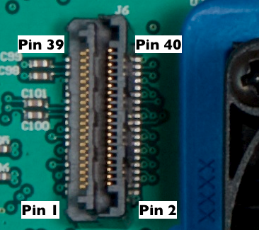
Take care in mapping pins between boards, across the orientation switch of the two LSHM connectors. The pinout and drawing below show the connector on the WARP v3 board.
Pin Connection 6, 8, 10, 12, 16, 18, 20, 22, 26, 28, 30, 32 CLKHDR_CTRL<0:11> 2.5v FPGA I/O (see UCF below) 7, 9, 11, 13 CLKHDR_CTRL<12:15> 2.5v FPGA I/O (see UCF below ) 17, 19 RF Reference Clock buffer CLKOUT0 23, 25 Sampling Clock buffer CLKIN2 29, 31 Sampling Clock buffer CLKOUT1 35, 37 RF Reference Clock buffer CLKIN2 36, 38 FPGA CC LVDS p/n pins (see UCF below) 1, 2, 3 3.3v (supplied by WARP v3 board, 500mA max) 4, 14, 15, 21, 24, 27, 33, 34, 39, 40 Ground
NOTE: The FPGA I/O connections routed to the clock module header support only 2.5v logic. The clock module must implement any necessary level shifting for other logic levels.
The UCF snippet for the clock module FPGA I/O connections is below.
NET "CLKHDR_CTRL<0>" LOC = "V34" | IOSTANDARD = "LVCMOS25";
NET "CLKHDR_CTRL<1>" LOC = "V33" | IOSTANDARD = "LVCMOS25";
NET "CLKHDR_CTRL<2>" LOC = "V27" | IOSTANDARD = "LVCMOS25";
NET "CLKHDR_CTRL<3>" LOC = "V28" | IOSTANDARD = "LVCMOS25";
NET "CLKHDR_CTRL<4>" LOC = "V32" | IOSTANDARD = "LVCMOS25";
NET "CLKHDR_CTRL<5>" LOC = "W34" | IOSTANDARD = "LVCMOS25";
NET "CLKHDR_CTRL<6>" LOC = "W30" | IOSTANDARD = "LVCMOS25";
NET "CLKHDR_CTRL<7>" LOC = "W29" | IOSTANDARD = "LVCMOS25";
NET "CLKHDR_CTRL<8>" LOC = "Y34" | IOSTANDARD = "LVCMOS25";
NET "CLKHDR_CTRL<9>" LOC = "Y33" | IOSTANDARD = "LVCMOS25";
NET "CLKHDR_CTRL<10>" LOC = "Y31" | IOSTANDARD = "LVCMOS25";
NET "CLKHDR_CTRL<11>" LOC = "Y32" | IOSTANDARD = "LVCMOS25";
NET "CLKHDR_CTRL<12>" LOC = "V30" | IOSTANDARD = "LVCMOS25";
NET "CLKHDR_CTRL<13>" LOC = "R34" | IOSTANDARD = "LVCMOS25";
NET "CLKHDR_CTRL<14>" LOC = "W26" | IOSTANDARD = "LVCMOS25";
NET "CLKHDR_CTRL<15>" LOC = "V29" | IOSTANDARD = "LVCMOS25";

NET "CLKHDR_FPGA_CC_N" LOC = "AE24" | IOSTANDARD = "LVDS_25" | DIFF_TERM = "TRUE";
NET "CLKHDR_FPGA_CC_P" LOC = "AD24" | IOSTANDARD = "LVDS_25" | DIFF_TERM = "TRUE";
The orientation and pin numbering of the clock module header on the WARP v3 board is illustrated in the figure below. Refer to the LSHM datasheet for details on which pins connect when two LSHM connectors are mated.
