| Version 6 (modified by murphpo, 12 years ago) (diff) |
|---|
WARP v3 User Guide: RF Interfaces
The WARP v3 board integrates two identical RF interfaces. The basic structure of each interface is illustrated below.

On the WARP v3 board and in our reference designs, these interfaces are labeled RF A and RF B, where RF A is nearer the top edge of the board (closer to the hex displays).
AD9963 ADC/DAC
The conversion between the analog I/Q and digital I/Q domains is handled by the Analog Devices AD9963 MxFE. The AD9963 integrates two 100MSps 12-bit ADCs, two 170MSps 12-bit DACs, interpolation and decimation filters and programmable analog gain and offset adjustments. Refer to the ADI AD9963 datasheet for full specifications.
The AD9963 is very flexible and includes a register bank to control various functions on the chip. The registers are accessed via a dedicated SPI interface. We have designed the w3_ad_controller core to access the AD9963 registers via the SPI interface.
The digital I/Q ports on the AD9963 operate at double data rate, with I/Q interleaved. We have designed the w3_ad_bridge core to connect these DDR ports to separate internal I/Q busses in user designs.
Tx Data Path
The AD9963 integrates 3 stages of digital interpolation filters. These filters can be en/disabled at run time via SPI register writes. By cascading the filters the AD9963 can apply interpolation of 1x, 2x, 4x or 8x.
A single AD9963 Tx data path is illustrated below. Identical data paths are implemented for both DACs (I and Q).
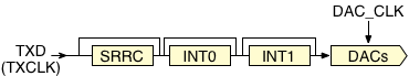
| Int Rate | Enabled Filters |
|---|---|
| 1 | None |
| 2 | INT0 |
| 4 | INT0, INT1 |
| 8 | INT0, INT1, SRRC |
The figures below show the effective frequency response of the Tx path for interpolation rates 2, 4, and 8. The frequency axis is normalized to the DAC sampling rate. These figures come from pg. 38 of the AD9963 datasheet.
| 2x Interpolation | 4x Interpolation | 8x Interpolation |
|---|---|---|
 |  | 
|
Clocking
The clocking configuration of the AD9963 is flexible and, as a result, complicated. There are to main clock domains in the AD9963: data clocks, connected to the FPGA, and converter clocks, used by the ADC/DAC cores.
The converter clocks are illustrated below.

Notice that the DAC and ADC clocks are always derived from the AD9963 reference clock input, not the data clock inputs. The data clocks must be synchronous to the converter clocks, but by separating these domains the low jitter of the original reference clock is preserved.
The DLL parameters (M/N), ADC clock divider and mux selects are all configured via SPI register writes.
MAX2829 Transceiver
The WARP v3 RF interfaces use the Maxim MAX2829 transceiver to translate between baseband and RF. The MAX2829 implements both 2.4 and 5GHz Tx/Rx paths. For full specifications refer to the MAX2829 datasheet.
The MAX2829 transceiver has a number of digital control lines and a dedicated SPI interface for internal register access. We have designed the radio_controller core to manage these control interfaces in user designs.
Each transceiver generates its own RF carrier signal, derived from a reference clock input. The reference clocks for both RF interfaces are driven by an AD9512 clock buffer (see for details). The MAX2829 requires either a 20MHz or 40MHz reference clock. The AD9512 must be configured to divide its 80MHz input to generate the desired reference frequency.
Power Amplifier
The WARP v3 design currently uses the Anadigics AWL6951 dual-band power amplifier. Every board is tested to ensure >20dBm output power at both 2.4 and 5GHz. Refer to the AWL6951 datasheet for full specifications.
RF Port
Each RF interface is connected to a 50 ohm SMA jack. This connector is a standard polarity, standard thread SMA jack. The SMA jack should always be terminated into a 50 ohm load. The WARP v3 kit includes SMA terminators for each RF interface. Users must supply their own RF cables or antennas to suit their application.
The maximum input power at the SMA connector should never exceed 0dBm, to avoid damage to the MAX2829 RF inputs.
The performance of the MAX2829 RF inputs are specified for input powers below approximately -10dBm. To connect two WARP v3 kits via a coax cable, ensure there is at lest 40dB series attenuation.