| Version 1 (modified by murphpo, 12 years ago) (diff) |
|---|
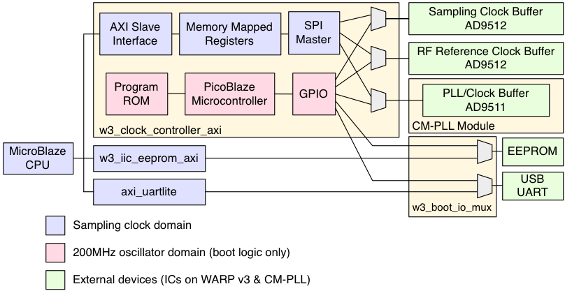
WARP v3 Clock Controller (w3_clock_controller)
This core implements an SPI master for reading/writing registers in the AD9512 clock buffers on the WARP v3 board. For details about how these buffers are connected to the FPGA and RF interfaces, refer to the WARP v3 User Guide Clocking section.
The w3_clock_controller core is packaged as a pcore which can instantiated in an XPS project. The design has been tested in hardware using Xilinx ISE 13.4.
Hardware
The WARP v3 board uses two AD9512 clock buffers: one for distributing the sampling clock (to the RF interfaces, FPGA and FMC slot) and one for distributing the RF reference clock (to the RF interfaces and FMC slot). The w3_clock_controller HDL implements parallel SPI interfaces, one per AD9512 buffer. There are 4 SPI pins per buffer which must be connected to the corresponding FPGA pins. Refer to the WARP v3 reference projects for examples of known-good hardware configurations.
Driver
The w3_clock_controller pcore includes a C driver to facilitate control of the AD9512s from user code. Refer to the w3_clock_controller driver documentation for more details.
All driver functions require the base memory address of the w3_clock_controller pcore. This address is set in your XPS project. The EDK tools copy this address into a macro in the xparameters.h file when you generate a BSP. The auto-generated macro should be named XPAR_W3_CLOCK_CONTROLLER_0_BASEADDR (assuming your pcore instance is named w3_CLOCK_controller_0, as in our reference projects).
//Define our own macro, in case EDK changes its naming scheme in the future
// Assumes pcore instance is named w3_ad_controller_0; confirm in xparameters.h
#define CLOCK_BASEADDR XPAR_W3_CLOCK_CONTROLLER_0_BASEADDR
Usage
An important factor in configuring the WARP v3 clock buffers is whether the FPGA logic implementing the w3_clock_controller core is itself clocked by the sampling clock. If so, it is critical the properties of the AD9512->FPGA clock are not changed by user code. All other outputs from the AD9512 buffers can be changed as needed by user code.
The w3_clock_controller driver provides functions to configure the AD9512 output dividers, thereby configuring the frequency of the clocks feeding the RF interface AD9963 chips (the ADC/DAC chips). It is critical that the AD9512->AD9963 clock frequency be consistent with all other rates in the FPGA->DAC and ADC->FPGA interfaces. The combination of AD9963 clock settings (DLL state, ADC/DAC clock source, etc.), AD9963 filter settings (interpolation/decimation rates), AD9512 dividers and internal FPGA->w3_ad_bridge clock connections must all agree. Refer to the WARP v3 User Guide RF section for more details and examples of valid AD9512/AD9963/FPGA configurations.
Source
The full hardware and software source code is available in the repository: PlatformSupport/CustomPeripherals/pcores/w3_clock_controller_v3_00_b. The VHDL, Verilog and C source code are made available under the WARP license.
Attachments (8)
- w3_clock_controller_block_diagram.png (81.2 KB) - added by murphpo 9 years ago.
- cmpll_dipsw_cfgsel_100.png (1.1 KB) - added by murphpo 9 years ago.
- cmpll_dipsw_cfgsel_101.png (1.1 KB) - added by murphpo 9 years ago.
- cmpll_dipsw_cfgsel_110.png (1.1 KB) - added by murphpo 9 years ago.
- cmpll_dipsw_cfgsel_111.png (1.1 KB) - added by murphpo 9 years ago.
- cmmmcx_sipsw_cfgsel_00.png (885 bytes) - added by murphpo 9 years ago.
- cmmmcx_sipsw_cfgsel_01.png (858 bytes) - added by murphpo 9 years ago.
- cmmmcx_sipsw_cfgsel_10.png (867 bytes) - added by murphpo 9 years ago.
Download all attachments as: .zip