Base System Builder - FPGA Board v2.2
This section describes the process of launching XPS and creating a simple hardware/software platform using Base System Builder. This section of the tutorial is specifically created for FPGA Board v2.2. Once you complete this, skip to XPS Intro - Implementing the hardware design. Use the previous section if you have FPGA Board v1.2.
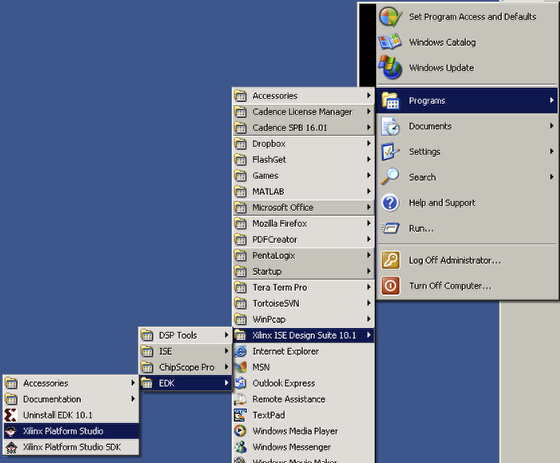
Launch Xilinx Platform Studio.
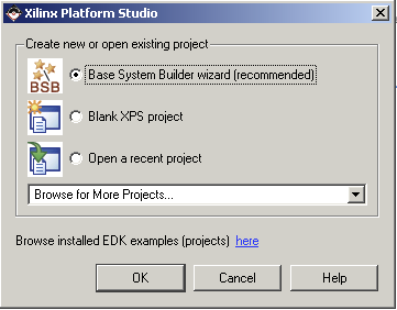
Select Base System Builder to create a new design.
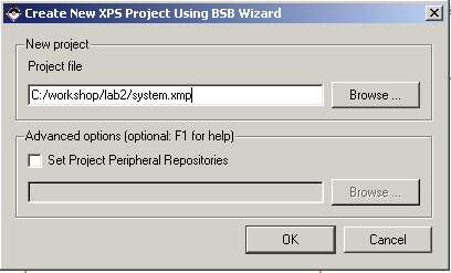
Enter a path for your project. Two key requirements:
-The project file must be named 'system.xmp'
-The project file must be saved to a folder with no spaces in its path - "C:\Documents and Settings\user\" will not work!
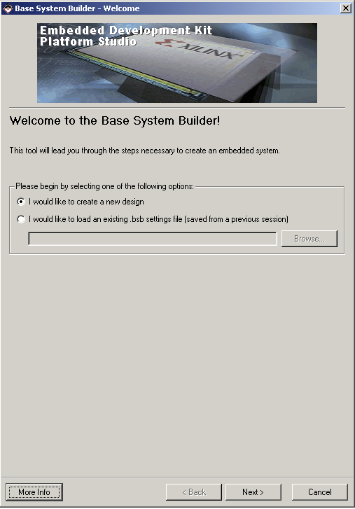
Choose the option for a new design.
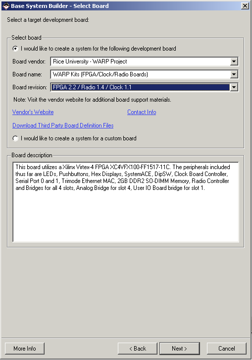
Select WARP Kits (FPGA/Clock/Radio Boards) and FPGA v2.2 / Radio 1.4 / Clock 1.1.
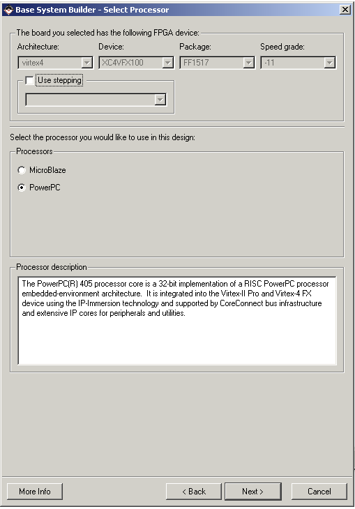
The Xilinx EDK supports two embedded processors. The PowerPC processor is a "hard" processor core, embedded in the fabric of the Virtex-4 FPGA on the WARP FPGA board. MicroBlaze is a "soft" processor core, implemented in the FPGA fabric itself. For this exercise (and all WARP designs generally), select the PowerPC core.
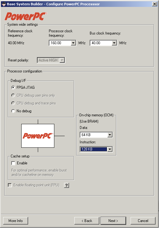
The clocking and memory architectures for EDK designs are very flexible. Base System Builder supports some simple clock/memory configurations. In more sophisticated designs, the clocking and memory options can be further customized by hand. For this exercise, select the clock frequencies and memory sizes shown above.
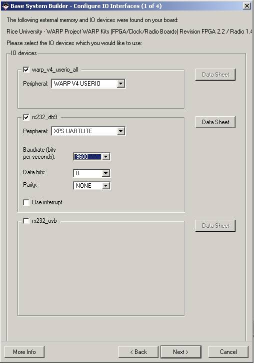
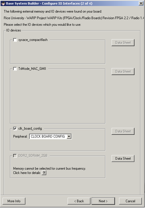
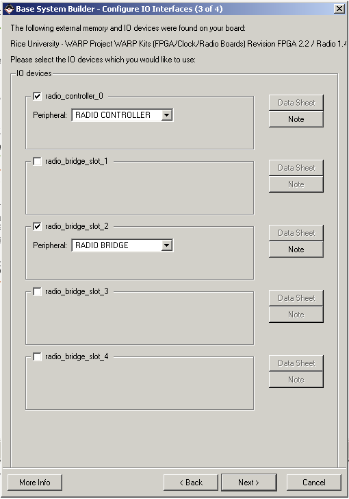
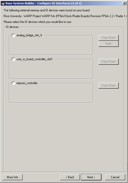
The next few screens present a list of available I/O devices. Each device corresponds to an off-chip interface on the WARP FPGA board. Each device can be enaled/disabled using its checkbox. For this exercise, choose the peripherals as follows:
Enabled:
- warp_v4_userio_all
- rs232_db9
- clock_board_config
- radio_bridge_slot_2
- radio_controller_0
Disabled:
- rs232_usb (a second serial port that is converted to USB on the board using an FTDI chip)
- sysace_compactflash
- TriMode_MAC_GMII
- DDR2_SDRAM_2GB
- radio_bridge_slot_1
- radio_bridge_slot_3
- radio_bridge_slot_4
- eeprom_controller
- analog_bridge_slot_4
- user_io_board_controller_slot1
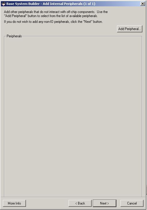
After configuring off-chip devices, you now configure on-chip peripheral cores. By default, an internal RAM block is enabled. For this exercise, click 'Remove' to omit this core from the design.
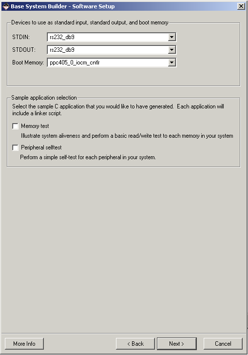
For user applications running in the PowerPC processor, the EDK tools can map the WARP FPGA board's serial port (the core named 'rs232_db9' here) to the STDIN/STDOUT conventions. This allows funcitons like printf() to work normally, using an external terminal emulator as the PowerPC's display and keyboard.
XPS can also create sample software projects which exercise the memory and peripheral devices in your hardware design. For this exercise, disable both example proejcts (you'll create a new software project later).
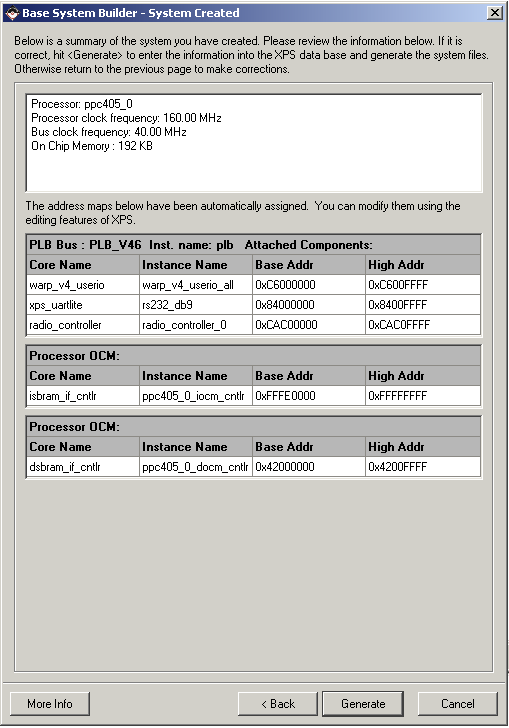
Base System Builder assigns default memory addresses to each memory and memory-mapped peripheral device. The addresses in your project may vary from those shown here. In general, the defaults selected by BSB work fine.
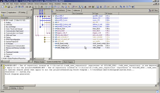
When Base System Builder finishes, XPS will open the resulting project. The remaining sections of this exercise describe how to use this interface to customize and test your hardware & software platform.