| Version 3 (modified by murphpo, 17 years ago) (diff) |
|---|
WARP FPGA Board Multi-Gigabit Transceivers
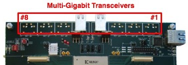
The FPGA board provides 8 multi-gigabit transceiver connections for board-to-board links. These transceivers are each capable of 3.125Gb/sec full-duplex communication with another board. The MGTs are provided to enable very high-speed connections between multiple WARP FPGA boards for applications requiring the processing resources of multiple FPGAs.
For extensive documentation on using the MGTs, refer to Xilinx's Virtex-II Pro MGT Users Guide.
The MGT connections are arrayed along the top of the FPGA board, numbered 1-8 right-to-left.
MGT Clocking
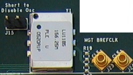
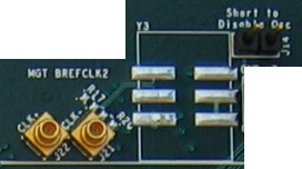
MGTs require reference clocks provided by very low jitter differential oscillators. The WARP FPGA board includes footprints for two such oscillators. One is mounted by default; the other is left unmounted for future customization.
The MGTs require clocks driven into specific pins on the FPGA, refered to as BREFCLK and BREFCLK2. The left oscillator (component Y1) drives BREFCLK; the right oscillator (component Y3) drives BREFCLK2. The pin mapping for these clock signals are:
| Clk Input | Schematic Name | FPGA Pin |
| BREFCLK+ | MGT_CLK0P | E20 |
| BREFCLK- | MGT_CLK0N | D20 |
| BREFCLK2+ | MGT_CLK1P | J20 |
| BREFCLK2- | MGT_CLK1N | K20 |
| BREFCLK Oscillator | BREFCLK2 Oscillator |
 | 
|
The oscillators can be disabled by mounting shunts on the adjascent 2-pin headers. When disabled, the reference clock can be driven to the FPGA through a pair of MMCX connectors. This allows multiple FPGA boards to share a common MGT reference clock, which enables an applicaiton to bypass the high-latency elastic buffers in the transceivers.
VTRX Configuration
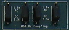
Short bottom pins for 2.5v (required for WARP board-to-board links), top pins for 1.8v (for connections to AC-coupled transmitters).

