| Version 7 (modified by murphpo, 18 years ago) (diff) |
|---|
WARP Daughtercard Specification
The WARP FPGA Board has four daughtercard slots. The four slots are electrically and mechanically identical. A daughtercard designed to meet the specifications below can be used in any of these slots.
Electrical Details
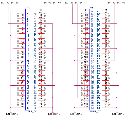
Each daughtercard slot consists of two 80-pin connectors on the FPGA board. 124 pins are routed to dedicated I/O on the FPGA. The remaining 36 signals are used for power and ground connections. On the Virtex-II Pro WARP FPGA board, each daughtercard slot is routed to a dedicated I/O bank on the FPGA. These I/O banks are configured for 3.3v single-eneded I/O and support 50Ω digitallly controlled impedence. The 36 power pins are split between ground (20 pins), +5v (12 pins) and -5v (4 pins). The ground pins are connected directly to the ground planes on the FPGA board. The +5v pins are connected to a dedicated 18A switching supply on the FPGA board. The -5v pins are connected to a header on the FPGA board which can be populated with an isolated supply when needed. The power pins on the four daughtercard slots are all connected together on the FPGA board.
See the WARP FPGA Board Schematics for the actual circuits implemented on the FPGA board.
Schematic
This is a schematic view of the 160-pin daughtercard slot. The connectors are represented by a heterogeneous part, each containing 80 pins. The 36 power pins are connected to ground, +5v and -5v (EXT_DGND, EXT_5v, EXT_-5v in the schematic). The source file for this schematic is available below.
Mechanical
WARP daughtercards must meet certain mechanical requirements. First, the two 80-pin connectors must be oriented, aligned and spaced to match the placement of the mating connectors on the FPGA board. Second, a mounting hole should be included to secure daughtercards to their slots. Finally, the PCB must not extend beyond certain dimensions in order to fit in the space allowed by the FPGA's heat sink and adjascent daughtercards.
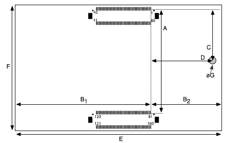
The drawing below is a daughtercard viewed from the top, oriented for slots #1 and #2 (with the FPGA board's left-edge at the left and the FPGA itself to the right). The connectors are mounted on the bottom of the daughtercard; the footprint included in this drawing is viewed from the top (i.e. through the board) as it is in PCB design tools.
- A = 1.471"; vertical distance from center of pin 1 to center of pin 81
- B1 = 1.923"; horizontal distance from left edge to pin 1/81 vertical
- B2 = 1.005"; horizontal distance from right edge to pin 1/81 vertical
- C = 0.735"; vertical distance from mounting hole center to pin 1
- D = 0.883"; horizontal distance from mounting hole center to pin 1/81 vertical
- E = 2.928"; horizontal edge to edge
- F = 1.780"; vertical edge to edge
- øG = 0.1" (diameter before plating); plated mounting hole (connected to ground)
A vector PDF version of this drawing is also available: Daughtercard Mechanical Drawing PDF.
WARP daughtercards use two 80 pin headers per daughtercard slot. The connectors are 0.5mm pitch, 4mm height headers with metal fittings from the Hirose DF17 series of connectors. The Hirose part number is DF17(4.0)-80DP-0.5V(57). See the Hirose DF17 Connectors Datasheet for the full mechanical details (pg 6) and recommended PCB footprint (pg 8).
The parts are available from Digikey; search for Digikey part number H11148CT-ND.
Reference Designs
Daughtercard_Template_Schematic.zip
Cadence Capture CIS 15.7 project, schematic design and parts library.
Daughtercard_Template_Board.zip
Cadence Allegro PCB Editor 15.7 padstacks, package symbols and sample board.

