CM-PLL Clock Module: Configuration
The CM-PLL circuits are configured by two elements:
- A 6-position DIP switch on the CM-PLL board
- SPI control of the AD9511 register bank
DIP Switch
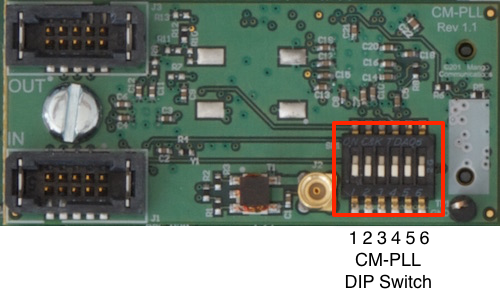
The figures below depict switch settings for the 6-position DIP switch on the CM-PLL. Refer to the photo below for the orientation and switch numbering used throughout this guide.

Reference Clock Output
Switch 1 controls the reference clock output pin on the external header:
| Switches | Configuration |
|---|---|
 | Disables the reference clock output. Use this configuration when no cable is connected to the OUT external header. |
 | Enables the reference clock output. Use this configuration when a cable is connected to the OUT external header and the downstream CM-PLL has selected its external header reference clock input. |
Reference Clock Source
Switches 2 and 3 control the reference clock mux:
| Switches | Configuration |
|---|---|
 | Selects the MMCX Jack reference clock input. Use this configuration when driving the reference clock from external equipment or from a CM-MMCX clock module on another WARP v3 kit. |
 | Selects the External Header reference clock input. Use this configuration when driving the reference clock from another CM-PLL clock module on another WARP v3 kit via the board-to-board headers. |
 | Selects the Local WARP v3 Oscillator reference clock input. Use this configuration when no external reference clock is required. This configuration should be used at the first node in a daisy chain of WARP v3 kits with CM-PLL modules. |
Application Specific Configuration
Switches 4-6 are connected to FPGA I/O. These switches do not directly affect any circuits on the CM-PLL board. The user-supplied FPGA design should read these switch values to configure clock modes at boot.
Refer to the w3_clock_controller documentation for details on the default use of these switches in the reference designs for WARP v3.
AD9511 SPI Control
The CM-PLL is built around the Analog Devices AD9511 PLL. The AD9511 is configured primarily via its internal register bank. Individual registers can be read and written via an SPI interface. The CM-PLL design connects this SPI interface to dedicated FPGA I/O. The AD9511 default register values do not result in a valid configuration for the WARP v3 + CM-PLL hardware. The user FPGA design must integrate an SPI controller to configure the AD9511 registers at boot. Refer to the AD9511 datasheet for details on the device's register bank.
We provide the w3_clock_controller core to manage the AD9511 interface from a MicroBlaze processor. This core also implements a standalone state machine to load configuration data into the AD9511 immediately following FPGA configuration, before the host MicroBlaze processor boots. This allows the MicroBlaze (and its interconnect and peripherals) to use clocks generated by the CM-PLL. The pre-boot configuration loaded by the w3_clock_controller core can be customized by writing configuration data to the WARP v3 EEPROM. Refer to the w3_clock_controller user guide for details.