Getting to Know the WARP v3 Hardware
In this section of the Getting Started guide, we offer information about the WARP v3 hardware and tips on how to protect the hardware from damage during operation. The material presented here supplements the complete WARP v3 Hardware Users Guide.
The Key Components of the Hardware
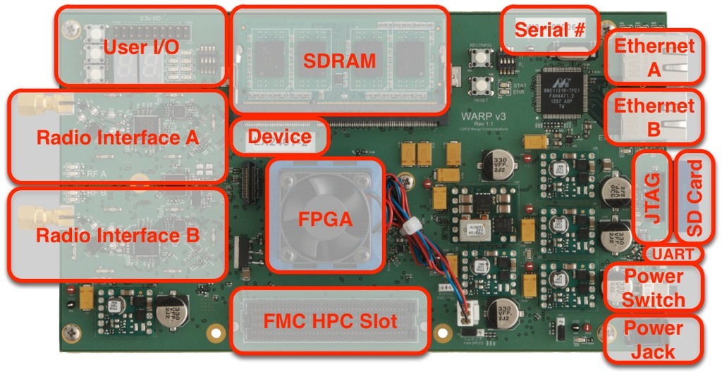
Throughout the documentation in this wiki and in the forums, we will refer to different components of the hardware by certain terminology and acronyms. In this section, we list these components along with a high-level description of what each component is responsible for.

- User I/O: This collection of push buttons, LEDs, hexadecimal displays, dip switches, and debug header pins is used for interacting with the board. Designs can read values from the switches and push buttons and can write values to the displays and LEDs. The debug header can be used for any number of purposes, such as providing a convenient way for one WARP board to trigger the action of another board over a wire.
- Radio Interfaces A & B: These interfaces provide the radios that allow designs to communicate at the 2.4GHz and 5GHz bands. For each radio interface, digital I and Q values from the FPGA are taken through digital-to-analog converters and are delivered to the transceiver for upconversion (i.e. wireless transmission). Wireless reception follows the reciprocal process where I and Q analog streams are taken from the transceiver through analog-to-digital conversion and are then delivered to the FPGA. The interfaces are labeled "RF A" and "RF B" on the board and in our reference designs.
- SDRAM: This DDR3 SO-DIMM provides extra memory beyond the block RAM inside the FPGA. The WARP v3 kit ships with a pre-tested 2GB SO-DIMM.
- Device label: This label shows the FPGA device on the WARP v3 board. This device is used in a number of places during the development process (such as exporting a peripheral core from Xilinx System Generator), so this label is present for convenient lookup.
- Virtex-6 FPGA: Under the fan, the FPGA serves as the central processing system for the WARP board.
- FMC HPC Slot: The FPGA Mezzanine Card High Pin Count slot provides connectivity to an existing ecosystem of hardware as well as future WARP-specific modules.
- Serial #: This is the unique serial number for the WARP board. This number is also programmed into an EEPROM on the board prior to shipping, allowing software running on the hardware to read this information.
- Ethernet A/B: The two 10/100/1000 Ethernet ports provide high-speed connectivity between the board and a wired network. The ports are labeled "ETH A" and "ETH B" on the WARP v3 board and in our reference designs.
- JTAG: The JTAG connector allows direct programming of the Virtex-6 FPGA using a Digilent or Xilinx JTAG cable.
- SD Card: An alternative to programming the board over JTAG is to use the SD card. This allows non-volatile storage of programs that will automatically download and execute upon insertion of the SD card.
- UART: The micro-USB connector on the board allows programs on the board to print messages to a terminal running on a computer.
- Power Switch: The power switch controls power to the board. The "off" position is where the switch is furthest away from the power jack. The "on" position is where the switch is closest to the power jack.
- Power Jack: The power jack is where the 12V power supply that comes with the WARP hardware should be plugged in. Note: the power switch should be in the "off" position whenever the power plug is inserted or removed. This allows the circuitry controlled by the switch to properly sequence the power regulators on the board.
Protecting your Hardware
WARP v3 is designed as a prototyping platform. As such, the hardware is shipped as an exposed board, with the various connectors and interfaces ready for access by user designs. This also means that sensitive circuits on the hardware are exposed and can be damaged by misuse. You must take care when handling the WARP v3 board.
Electrostatic Discharge Protection
On many pages in this wiki, you may see this warning:
 | The WARP v3 board is sensitive to electrostatic discharge (ESD). You must take ESD precautions when handling the hardware. Always ensure you are grounded before touching the board. Damage due to ESD is not covered by warranty. |
Always make sure you are grounded before handling hardware. We recommend storing unused kits in the original anti-static packaging. When using the hardware, we recommend using proper ESD protection devices (grounded wrist straps, etc.).
Overheating Protection
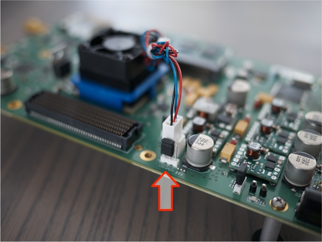
The Xilinx Virtex-6 FPGA can generate significant amounts of heat when running complex designs. It is important that the supplied fan be running whenever the board is in use. For the fan to run, a jumper needs to be present.

Each board will be shipped with this jumper connected. This jumper should not be removed. Verify that it is present before using the board.
Radio Protection
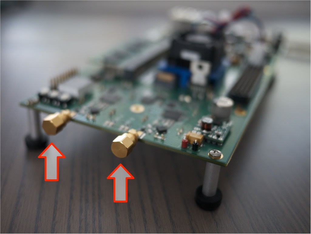
Always ensure the SMA connector is terminated into a 50 ohm load before powering on the board. Whenever the radios are not in use, they should be terminated with the included 50 ohm SMA terminators.

These terminators should be removed when an antenna or RF cable are connected.
Installing an FMC Module
WARP v3 includes a FMC HPC slot which can host an FMC module (a.k.a. FMC daughtercard). The FMC connector requires considerable force to mate and separate boards. It is essential you brace the WARP v3 board when mounting/removing FMC modules, to avoid flexing the PCB and breaking solder joints under the FMC connector and FPGA.
The video below shows the proper technique for connecting an FMC module. Do not simply press the FMC module down. Always prevent flexing the WARP board by pinching the FMC module and the WARP board together.
Removing an FMC Module
Similarly, removing an FMC module requires bracing the WARP board to prevent flexing.
The video below shows the proper technique for removing an FMC module.