WARP Radio Board Clocking
There are three clock domains on the Radio Board, as described below.
RF Reference Clock
The MAX2829 transceiver requires a refence clock which is multipled up by its PLL to form the RF carrier. This must be a 20MHz or 40MHz clock and must be driven into the Radio Board's MMCX jack. In standard WARP kits, the WARP Clock Board drives this signal at 20MHz. If multiple Radio Boards are driven by the same RF reference clock, their RF carriers will be synchronous, though there will be a phase offset resulting from their PLLs locking at different times.
I/Q Sampling Clock
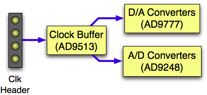
The I/Q ADCs and DACs are driven by a common clock. This clock is produced on an on-board clock buffer (an Analog Devices AD9513). The source clock for this buffer comes from an off-board source driven into a 4-pin connector. In standard WARP kits, the WARP Clock Board drives this signal at 40MHz. If multiple Radio Boards are used on a single kit, they should all be driven by synchronous and in-phase sampling clocks.
RSSI Sampling Clock
The dedicated RSSI ADC is clocked from the FPGA via the daughtercard headers. Any frequency up to 20MHz is valid. There is no requirement for this clock to be synchronous with other clocks on the Radio Board.


