WARPLab 7
- Downloads
Getting Started
- Sample Buffer Sizes
- Automatic Gain Control
- Examples
- Extending WARPLab
- Debugging Errors
- Porting Code
- Benchmarks
WARPLab 7 Framework
WARPLab 7 Reference Design
Reference Design Modules
- Node
Interface Group
Baseband
Transport
Trigger Manager
Hardware
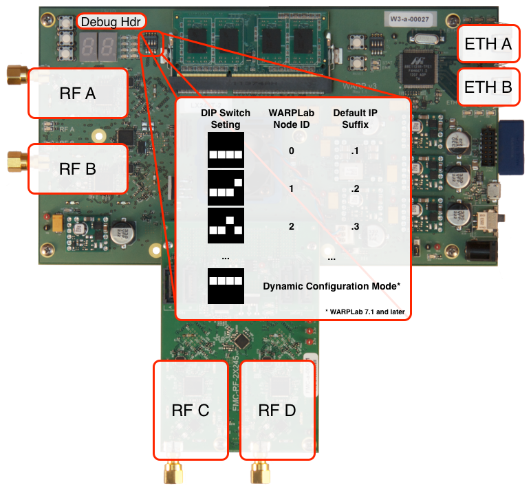
WARPLab Reference Design Hardware Config: WARP v3

Radio Interface
- In the 2 RF Node configuration (ie only RF A and RF B are populated), you should only use the 2RF bitstream in the download.
- In the 4 RF Node configuration (ie all RF interfaces are populated), you should only use the 4RF bitstream in the download.
Dip Switches
- In WARPLab 7.1 and later, the dip switch value of 0xF (ie all switches set to '1'), is reserved for dynamic node configuration.
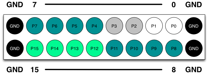
Debug Header
Updated for WARPLab 7.5
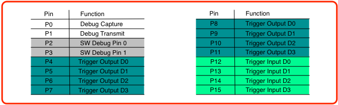
The debug header is configured by default to map to the following pins:

 | These pins are not 3.3v compatible! You must use external level shifting to interface with non-2.5v signals. |

NOTE: The Debug Header is defined in the system.ucf and the connections are defined in the system.mhs
- The Trigger output and Trigger input pins above are used with the Trigger Manager
- The CM-PLL Clock Module shares FPGA I/O between boards as well as a clock reference. This allows easy node synchronization with a single cable. In WARPLab 7.5, the 4 trigger outputs are duplicated and sent to both the CM-PLL board as well as the debug header. The 4 trigger inputs are digitally ORed from pins connecting both the CM-PLL board as well as the debug header.
- For WARPLab 7.6.0 and above, the trigger input / output IDs from the trigger manager are as follows:
Trigger Output D0  == EXT_OUT_P0
Trigger Output D1  == EXT_OUT_P1
Trigger Output D2  == EXT_OUT_P2
Trigger Output D3  == EXT_OUT_P3
Trigger Input  D0  == EXT_IN_P0
Trigger Input  D1  == EXT_IN_P1
Trigger Input  D2  == EXT_IN_P2
Trigger Input  D3  == EXT_IN_P3
Clock Configuration
Updated for WARPLab 7.5
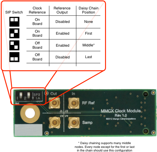
The WARPLab reference design does not require any external clock connections. By default the reference design will use the oscillators on the WARP v3 board for all system and RF clocking. The reference design does support both sourcing and sinking external clocks for synchronization of multiple nodes. There are two hardware options for this synchronization: the CM-MMCX Clock Module and the CM-PLL Clock Module
The CM-MMCX is capable of sourcing and/or sinking RF and sampling clocks. This clock module can be used in a daisy chain configuration, where a single primary node shares its internal clocks with a chain of secondary nodes that adopt and forward the clocks. The role of each node is configured via the 2-position SIP switch on the CM-MMCX, according to the figure below.
- Detailed information on the WARP v3 Clocking configuration can be found here.
- To adjust the functionality, please use the following SIP switch settings:

NOTE: The definition of the SIP switch settings for the CM-MMCX module changed between WARPLab 7.4.0 and earlier and WARPLab 7.5.0 and later. You can find the previous definition of the SIP switch settings here. Also, as part of the boot sequence, the node will print the clock configuration to the UART if there is any confusion about the settings.
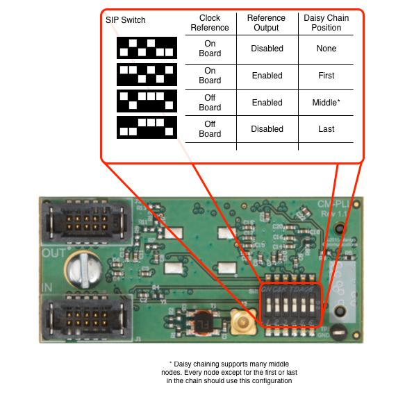
The CM-PLL is capable of sourcing and/or sinking a clock referenced used to discipline a PLL on each node. This clock module can be used in a daisy chain configuration, where a single primary node shares its clock reference with a chain of secondary nodes that adopt and forward the clock reference. The role of each node is configured via the 6-position SIP switch on the CM-PLL, according to the figure below.
- The CM-PLL also carries the four trigger inputs and four trigger outputs between nodes. The trigger inputs are ORed with the trigger inputs from the debug header. The trigger outputs are replicated versions of the debug header trigger outputs.
 In WARPLab 7.5.x, there is a bug in the mapping of trigger outputs in the CM-PLL connection: EXT_OUT_P0 is swapped with EXT_OUT_P2. See this forum post for more information.
- Detailed information on the WARP v3 Clocking configuration can be found here.
- To adjust the functionality, please use the following SIP switch settings:

Ethernet
- By default, only Ethernet connection A (Eth A) is used.
Attachments (5)
- WARP_v3_labelled.png (582.9 KB) - added by welsh 11 years ago.
- Debug_Header_Diagram.png (43.2 KB) - added by chunter 9 years ago.
- MMCX_v1_labelled.png (193.2 KB) - added by chunter 9 years ago.
- Debug_Header_Connections.png (38.1 KB) - added by chunter 9 years ago.
- PLL_v1_labelled.png (248.6 KB) - added by welsh 9 years ago.
Download all attachments as: .zip