WARP v3 AD Bridge (w3_ad_bridge)
The w3_ad_bridge core implements the I/O logic for interfacing user designs with the digital I/Q interfaces of the AD9963 ADCs/DACs on the WARP v3 board. The AD9963 digital ports are double data rate (DDR) interfaces with interleaved I/Q. The w3_ad_bridge core uses IDDR and ODDR primitives in the FPGA IOBs to efficiently translate between the external interleaved I/Q ports and internal separate I/Q busses. One w3_ad_bridge instance implements the digital interface for two RF paths.
The w3_ad_bridge core is packaged as a pcore which can instantiated in an XPS project. The design has been tested in hardware using Xilinx ISE 13.4. The w3_ad_bridge core does not attach to a processor bus, so there is no driver.
The current version of the w3_ad_bridge core is v3_00_g.
Refer to the latest WARP v3 reference projects for the recommended instantiation of the w3_ad_bridge core.
Tx Path
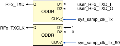
The w3_ad_bridge Tx path is illustrated below. The logic depicted here is replicated for each RF interface (RF A and RF B).

External Ports:
| Port | Direction | Width | Connection | Description |
|---|---|---|---|---|
| ad_RFA_TXD | Output | 12 | AD9963 TXD | RF A Tx data (DDR, I/Q interleaved) |
| ad_RFA_TXCLK | Output | 1 | AD9963 TXCLK | RF A Tx data clock |
| ad_RFA_TXIQ | Output | 1 | AD9963 TXIQ | RF A Tx data select (ignored in DDR mode) |
| ad_RFB_TXD | Output | 12 | AD9963 TXD | RF B Tx data (DDR, I/Q interleaved) |
| ad_RFB_TXCLK | Output | 1 | AD9963 TXCLK | RF B Tx data clock |
| ad_RFB_TXIQ | Output | 1 | AD9963 TXIQ | RF B Tx data select (ignored in DDR mode) |
Internal Ports:
| Port | Direction | Width | Description |
|---|---|---|---|
| sys_samp_clk_Tx | Input | 1 | Clock for user-supplied TXD signals |
| sys_samp_clk_Tx_90 | Input | 1 | 90 degree phase shifted version of sys_samp_clk_Tx |
| user_RFA_TXD_I | Input | 12 | RF A Tx I samples from user design |
| user_RFA_TXD_Q | Input | 12 | RF A Tx Q samples from user design |
| user_RFA_TXIQ | Input | 1 | RF A Tx I/Q select (ignored in DDR mode) |
| user_RFB_TXD_I | Input | 12 | RF B Tx I samples from user design |
| user_RFB_TXD_Q | Input | 12 | RF B Tx Q samples from user design |
| user_RFB_TXIQ | Input | 1 | RF B Tx I/Q select (ignored in DDR mode) |
TXCLK
The AD9963 TXCLK input is used to capture the data presented on the TXD bus. In order to meet setup/hold requirements, the FPGA TXCLK output is a 90-degree phase shifted version of the clock signal for the TXD output. The TXCLK output is generated using the same IOB ODDR primitives as the TXD outputs. This design minimizes skew between the TXD and TXCLK signals.
The user design must supply both sys_samp_clk_Tx and sys_samp_clk_Tx_90, assuring they are 90 degrees out of phase and synchronous to the input I/Q signals.
TXIQ
The TXIQ ports are used by the AD9963 to de-interleave I/Q when the TXCLK runs at 2x the TXD data rate. The w3_ad_bridge implements a passthrough from user_RFx_TXIQ to ad_RFx_TXIQ.
Our projects configure TXCLK to run at 1x the TXD data rate (i.e. DDR), so the TXIQ signal is not needed to de-interleave I/Q. The user_RFx_TXIQ ports are tied to GND in our reference projects.
Rx Path

External Ports:
| Port | Direction | Width | Connection | Description |
|---|---|---|---|---|
| ad_RFA_TRXD | Input | 12 | AD9963 TRXD | RF A Rx data (DDR, I/Q interleaved) |
| ad_RFA_TRXCLK | Input | 1 | AD9963 TRXCLK | RF A Rx data clock |
| ad_RFA_TRXIQ | Input | 1 | AD9963 TRXIQ | RF A Rx data select (ignored in DDR mode) |
| ad_RFB_TRXD | Input | 12 | AD9963 TRXD | RF B Rx data (DDR, I/Q interleaved) |
| ad_RFB_TRXCLK | Input | 1 | AD9963 TRXCLK | RF B Rx data clock |
| ad_RFB_TRXIQ | Input | 1 | AD9963 TRXIQ | RF B Rx data select (ignored in DDR mode) |
Internal Ports:
| Port | Direction | Width | Description |
|---|---|---|---|
| sys_samp_clk_Rx | Input | 1 | Clock for user I/Q outputs |
| user_RFA_RXD_I | Output | 12 | RF A Rx I samples for user design |
| user_RFA_RXD_Q | Output | 12 | RF A Rx Q samples for user design |
| user_RFB_RXD_I | Output | 12 | RF B Rx I samples for user design |
| user_RFB_RXD_Q | Output | 12 | RF B Rx Q samples for user design |
Clocks
The IDDR registers are clocked by the AD9963-generated TRXCLK. The IDDR outputs are re-registered through D flip flops clocked by the user-supplied sys_samp_clk_Rx. The user design must assure the AD9963 is configured to generate a TRXCLK at the same frequency as the user-supplied sys_samp_clk_Rx.
Source
The full hardware and software source code is available in the repository: PlatformSupport/CustomPeripherals/pcores/w3_ad_bridge_v3_00_g. The VHDL, Verilog and C source code are made available under the WARP license.
Changelog
2012-Aug-12:
- Created w3_ad_bridge_v3_00_g, branched from w3_ad_bridge_v3_00_f
- Separate sys_samp_clk ports for Tx/Rx paths, to enable different ADC/DAC data rates