WARP v3 User I/O Controller (w3_userio)
This core provides software access to the various user I/O resources on the WARP v3 board. These resources include the 12 user LEDs, 2 hex displays, 3 push buttons, and 4-position DIP switch. For details on the user I/O devices, refer to the WARP v3 User Guide.
The w3_userio core is packaged as a pcore with both custom HDL and a C driver.
Hardware
The w3_userio HDL implements a PLBv46 slave interface with multiple registers accessible from user code. Refer to the driver documentation below for details on setting these registers.
User Outputs
User outputs (LEDs, hex displays) can be controlled either from software or via hardware ports. The w3_userio core implements a 2-to-1 mux for each output bit:
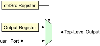
There is one bit in a usr_ port for each LED and hex display segment. The table below lists the w3_userio usr_ input ports. User logic should drive the ports corresponding to outputs configured for hardware control. When an output is configured for software control the corresponding usr_ port bit is ignored.
| Port Name | Width | Description |
|---|---|---|
| usr_hexdisp_left | 7 | Left hex display |
| usr_hexdisp_left_dp | 1 | Left hex display decimal point |
| usr_hexdisp_right | 7 | Right hex display |
| usr_hexdisp_right_dp | 1 | Right hex display decimal point |
| usr_leds_red | 4 | Red LEDs |
| usr_leds_green | 4 | Green LEDs |
| usr_rfa_led_red | 1 | Red LED near RF A |
| usr_rfa_led_green | 1 | Green LED near RF A |
| usr_rfb_led_red | 1 | Red LED near RF B |
| usr_rfb_led_green | 1 | Green LED near RF B |
By default only the RF LEDs are configured for hardware control. The control source of each output can be changed at anytime from user code.
Hex Display Mapping
The w3_userio core implements logic to map 4-bit values to the nearest 7-segment pattern for the corresponding hexadecimal digit. When enabled only the 4 LSB of the user-supplied value is used to update each hex display. When this logic is disabled the full 7-bit value is driven directly to the seven LED segments on the corresponding hex display. The mapping mode of each display can changed at any time from user code. Refer to the driver documentation below for details.
The 4-bit to 7-segment mapping logic is only available when the corresponding hex display is configured for software control. When configured for hardware control the 7-bit usr_ port is tied directly to the corresponding hex display outputs.
User Inputs
User inputs are debounced in HDL, with the debounced values captured in software-accessible registers. The debounced values are also driven to usr_ ports for use by custom logic. The table below lists the ports for each input device.
| Port Name | Width | Description |
|---|---|---|
| usr_dipsw | 4 | DIP switch |
| usr_pb_u | 1 | Up push button |
| usr_pb_m | 1 | Middle push button |
| usr_pb_d | 1 | Down push button |
FPGA DNA
The Virtex-6 FPGA implements a "DNA" feature, which provides a 56-bit value unique to every chip. This value is set at the factory and cannot be changed. User logic must instantiate the DNA_PORT primitive to access the DNA value. The w3_userio core implements logic to read the DNA value and capture it in a software-accessible register. This logic is implemented when the INCLUDE_DNA_READ_LOGIC parameter is set to 1.
When the DNA_PORT logic is included, the user design must provide a clock signal at the w3_userio DNA_Port_Clk port. This signal must be slower than 100MHz. If the DNA_PORT logic is omitted (i.e. INCLUDE_DNA_READ_LOGIC = 0) the DNA_Port_Clk port is ignored.
Instantiating the Core
The MHS snippet below shows the w3_userio instantiation used in the WARP v3 reference projects. The memory address is intentionally invalid; you must run "Generate Addresses" after adding the core.
Note that in this example four usr_ ports are used to provide hardware control of the RF LEDs. The signals connected to these ports (RFx_statLED_*) are driven by the radio_controller to indicate Tx/Rx status of each RF interface.
#Top level ports
...
# User I/O pins
 PORT USERIO_hexdisp_left_pin = USERIO_hexdisp_left_pin, DIR = O, VEC = [0:6]
 PORT USERIO_hexdisp_right_pin = USERIO_hexdisp_right_pin, DIR = O, VEC = [0:6]
 PORT USERIO_hexdisp_left_dp_pin = USERIO_hexdisp_left_dp_pin, DIR = O
 PORT USERIO_hexdisp_right_dp_pin = USERIO_hexdisp_right_dp_pin, DIR = O
 PORT USERIO_leds_red_pin = USERIO_leds_red_pin, DIR = O, VEC = [0:3]
 PORT USERIO_leds_green_pin = USERIO_leds_green_pin, DIR = O, VEC = [0:3]
 PORT USERIO_rfa_led_red_pin = USERIO_rfa_led_red_pin, DIR = O
 PORT USERIO_rfa_led_green_pin = USERIO_rfa_led_green_pin, DIR = O
 PORT USERIO_rfb_led_red_pin = USERIO_rfb_led_red_pin, DIR = O
 PORT USERIO_rfb_led_green_pin = USERIO_rfb_led_green_pin, DIR = O
 PORT USERIO_dipsw_pin = USERIO_dipsw_pin, DIR = I, VEC = [0:3]
 PORT USERIO_pb_u_pin = USERIO_pb_u_pin, DIR = I
 PORT USERIO_pb_m_pin = USERIO_pb_m_pin, DIR = I
 PORT USERIO_pb_d_pin = USERIO_pb_d_pin, DIR = I
 PORT dbg_hdr_gpio = dbg_hdr_gpio, DIR = IO, VEC = [15:0]
...
BEGIN w3_userio_axi
 PARAMETER INSTANCE = w3_userio
 PARAMETER HW_VER = 1.01.a
 PARAMETER INCLUDE_DNA_READ_LOGIC = 0
 PARAMETER C_BASEADDR = 0xFFFFFFFF
 PARAMETER C_HIGHADDR = 0x00000000
 BUS_INTERFACE S_AXI = mb_shared_axi_periph
 PORT S_AXI_ACLK = clk_160MHz
 PORT leds_red = userio_leds_red
 PORT leds_green = userio_leds_green
 PORT hexdisp_left = userio_hexdisp_left
 PORT hexdisp_right = userio_hexdisp_right
 PORT hexdisp_left_dp = userio_hexdisp_left_dp
 PORT hexdisp_right_dp = userio_hexdisp_right_dp
 PORT rfa_led_red = userio_rfa_led_red
 PORT rfa_led_green = userio_rfa_led_green
 PORT rfb_led_red = userio_rfb_led_red
 PORT rfb_led_green = userio_rfb_led_green
 PORT dipsw = userio_dipsw_b0 & userio_dipsw_b1 & userio_dipsw_b2 & userio_dipsw_b3
 PORT pb_u = userio_pb_u
 PORT pb_m = userio_pb_m
 PORT pb_d = userio_pb_d
 PORT usr_rfa_led_red = RFA_statLED_Rx
 PORT usr_rfa_led_green = RFA_statLED_Tx
 PORT usr_rfb_led_red = RFB_statLED_Rx
 PORT usr_rfb_led_green = RFB_statLED_Tx
 PORT usr_leds_red = dbg_signal_err_disp
END
...
Driver
The w3_userio pcore includes a C driver to access user I/O devices from user code. Refer to the w3_userio API documentation for full details.
All driver functions require the base memory address of the w3_userio pcore. This address is set in your XPS project. The EDK tools copy this address into a macro in the xparameters.h file when you generate a BSP. The auto-generated macro should be named XPAR_W3_USERIO_0_BASEADDR (assuming your pcore instance is named w3_userio_0, as in the example above).
The example below illustrates using the w3_userio driver from user code. Note that the core requires no initialization for normal operation.
//Define our own macro, in case EDK changes its naming scheme in the future
// Assumes pcore instance is named w3_userio_0; confirm in xparameters.h
#define USERIO_BASEADDR XPAR_W3_USERIO_0_BASEADDR

//Default state on reset:
//Select software control of all outputs except RF LEDs
//Set both hex dipslays to map 4-bit to 7-segment values
userio_write_control(USERIO_BASEADDR, (W3_USERIO_CTRLSRC_LEDS_RF | W3_USERIO_HEXDISP_L_MAPMODE | W3_USERIO_HEXDISP_R_MAPMODE));

//Display "B" on the left hex dipslay (assumes map mode is enabled; see control register docs)
userio_write_hexdisp_left(USERIO_ADDR, 0xB);

//Display "4" on the right hex dipslay and light the decimal point (assumes map mode is enabled; see control register docs)
userio_write_hexdisp_right(USERIO_ADDR, (0x4 | W3_USERIO_HEXDISP_DP) );

//Turn off all four green user LEDs
userio_write_leds_green(USERIO_ADDR, 0);

//Toggle the 2 LSB of the red user LEDs
userio_toggle_leds_red(USERIO_ADDR, 0x3);

//Check if middle push button is being pressed
if(userio_read_inputs(USERIO_BASEADDR) & W3_USERIO_PB_M) {...}

//Read 4-bit DIP switch value
u8 x = userio_read_inputs(USERIO_BASEADDR) & W3_USERIO_DIPSW;
Source
The full hardware and software source code is available in the repository: PlatformSupport/CustomPeripherals/pcores/w3_userio_axi_v1_02_a. The VHDL, Verilog and C source code are made available under the WARP license.