WARPLab 7
- Downloads
Getting Started
- Sample Buffer Sizes
- Automatic Gain Control
- Examples
- Extending WARPLab
- Debugging Errors
- Porting Code
- Benchmarks
WARPLab 7 Framework
WARPLab 7 Reference Design
Reference Design Modules
- Node
Interface Group
Baseband
Transport
Trigger Manager
Hardware
WARPLab 7 Example: Multi-Node Synchronization
File: wl_example_siso_txrx_nodeSync.m
This WARPLab example illustrates how to share clocks and triggers among WARP nodes to eliminate all timing and frequency offsets. This configuration has many uses. For example, when developing a new PHY it can be helpful to test performance with zero carrier frequency offset (CFO). This same configuration can also be used to synchronize multiple nodes for large-scale MIMO experiments, where the RF interfaces of multiple nodes are used together to form a meta node with many antennas.
This example uses two nodes. One acts as the source for clocks and triggers. The other acts as the sink. The source/sink relationship only applies to the synchronization signals. Both nodes can transmit and receive normally.
Setup
Requirements:
- WARPLab reference design 7.1.0 or later
- 2 WARP v3 nodes
- Clock connection between WARP boards. Either
- CM-MMCX assembly:
- 2 CM-MMCX clock modules (one per WARP v3 node)
- 2 MMCX cable assemblies
- 1 twisted pair cable assembly
- CM-PLL assembly:
- 2 CM-PLL clock modules (one per WARP v3 node)
- 1 CM-PLL compatible cable
- CM-MMCX assembly:
To run this example, you must setup your experiment as follows:
- Mount the CM-MMCX or CM-PLL modules on each WARP v3 node. Power must be off when mounting/unmounting a clock module.
- Set the CM-MMCX or CM-PLL switches on each node (see Clock Configuration settings); one node will be the clock source, the other will be the clock sink.
- Connect clock modules:
- If using the CM-MMCX modules, connect MMCX cables from the outputs of the source node to the inputs of the sink node. Then, connect the twisted pair cable between the debug headers of the WARP v3 boards. Pin 8 of the source node should connect to pin 15 of the sink node. Use the other conductor of the cable to connect ground between nodes (see this figure; note that this example does not require FMC-RF-2X245 modules).
- If using the CM-PLL modules, connect the cable between the Board-to-board Header Out of the source node and the Board-to-board Header In of the sink node.
- Set the DIP switches on the WARP v3 boards to 0000 (source node) and 0001 (sink node).
- Power on the WARP v3 nodes
- Download the WARPLab reference bitstream to both nodes (source node first). Both nodes should boot, with the source node showing "01" on the hex displays and the sink showing "02".
Please refer to the WARPLab Hardware Configuration user guide for more details on each of these steps.
Once the hardware is connected and programmed you can run the example m code: wl_example_siso_txrx_nodeSync.m.
Observations
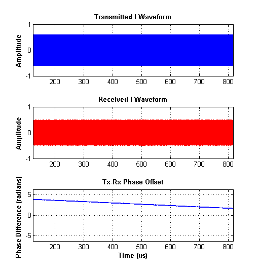
The wl_example_siso_txrx_nodeSync script creates a figure with three plots:
- Real part of the transmitted signal
- Real part of the received signal
- Phase difference (unwrapped) between the transmitted and received signals
When you run the script using fully synchronized nodes, the plot will look like this:
Note the constant phase difference between the Tx/Rx waveforms. If you re-run the script, this constant value will change. This is due to the RF transceivers being reset, which forces the PLLs to re-tune, leading to a new random phase offset between their RF carrier signals. If you skip the reset, the inter-radio phase offset will remain constant. You can observe this effect by commenting out the call to wl_initNodes() in the script (after running the script at least once).
If you disable the sharing of clock signals between nodes (by de-asserting both CM-MMCX switches at the sink node and re-programming the FPGA), you can directly observe the carrier frequency offset between the RF transceivers. The resulting plot will show a constant slope for the Tx-to-Rx phase difference. The CFO is proportional to this slope. The figure below illustrates this.
Attachments (6)
- nodeSync_hwCfg_sink.jpg (259.3 KB) - added by murphpo 11 years ago.
- nodeSync_hwCfg_source.jpg (241.6 KB) - added by murphpo 11 years ago.
- nodeSync_CFO.png (7.2 KB) - added by murphpo 11 years ago.
- nodeSync_constPhaseOffset.png (6.9 KB) - added by murphpo 11 years ago.
- SIP_clock_sink.png (9.3 KB) - added by welsh 11 years ago.
- SIP_clock_source.png (9.4 KB) - added by welsh 11 years ago.
Download all attachments as: .zip

