WARP User I/O Board | Trackball & Buttons
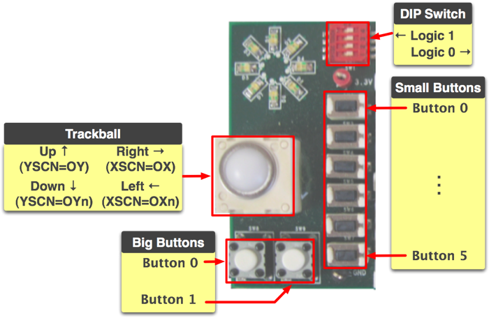
The user I/O board provides three kinds of input- a trackball, push buttons and a DIP switch. These components are shown here and described in detail below.
Trackball
The trackball is supplied by SparkFun Electronics. SparkFun also hosts a copy of the original datasheet.
The trackball contains five mechanical switches and has 8 pins tied to FPGA I/O via the daughtercard headers. The switches and their corresponding pins are illustrated below.
When the user scrolls the trackball up/down/left/right, the corresponding direction's switch alternates between closed and open. The switches for each axis (X and Y) share a common pin (XSCN and YSCN). The FPGA should drive these common pins high. The other pins are pulled low by discrete resistors on the User I/O Board. The FPGA can monitor these pins for a logic 1 to detect scrolling.
The trackball also has a switch to detect when the ball is pushed. This switch is normally open; when closed, it shorts pins SEL1 and SEL2. SEL1 should be driven high by the FGPA. SEL2 is pulled low and will show a logic 1 when the trackball is pushed.
The trackball input signals are debounced in hardware with simple RC circuits. It is recommended that user designs employ digital debouncing as well.
The pinout information for each button is listed below. The FPGA pins listed here correspond to WARP FPGA Board v1.2.
Trackball - Pinout
| Signal | Header Pin | Slot 1 Pin | Slot 2 Pin | Slot 3 Pin | Slot 4 Pin |
| XSCN | 87 | V4 | AN7 | AF33 | M32 |
| OX | 88 | V9 | AE12 | AG39 | L36 |
| OXn | 89 | U10 | AL9 | AJ39 | N31 |
| YSCN | 95 | T3 | AL6 | AE34 | N30 |
| OY | 94 | U9 | AN6 | AJ37 | L37 |
| OYn | 92 | T11 | AG9 | AH36 | L35 |
| SEL1 | 93 | U4 | AK8 | AC30 | M33 |
| SEL2 | 90 | V6 | AM7 | AJ38 | L38 |
Push Buttons
There are 8 discrete push buttons on the User I/O Board. Six are miniture buttons along the left edge of the LCD screen. These buttons are ideal for applications where the LCD is used interactively. Two larger push buttons are provided for general use. All 8 buttons are tied to dedicated FPGA I/O via the daughtercard headers.
Each button is debounced in hardware with a simple RC circuit. It is recommended that user designs employ digital debouncing as well.
The pinout information for each button is listed below. The FPGA pins listed here correspond to WARP FPGA Board v1.2.
Big Buttons - Pinout
| Button | Header Pin | Slot 1 Pin | Slot 2 Pin | Slot 3 Pin | Slot 4 Pin |
| 0 | 118 | P3 | AL2 | AD34 | P39 |
| 1 | 119 | R2 | AK3 | AL39 | P37 |
Small Buttons - Pinout
| Button | Header Pin | Slot 1 Pin | Slot 2 Pin | Slot 3 Pin | Slot 4 Pin |
| 0 | 118 | P3 | AL2 | AD34 | P39 |
| 1 | 63 | L5 | AF5 | AE30 | V39 |
| 2 | 64 | M7 | AD8 | AH30 | R32 |
| 3 | 65 | N2 | AK1 | AM34 | T34 |
| 4 | 67 | R11 | AF6 | AF29 | T30 |
| 5 | 68 | M2 | AE7 | AH29 | U36 |
DIP Switch
The four position DIP switch provides four independent switches, each tied to a dedicated FPGA input. When the switch is pushed right (away from the LEDs), the FPGA will observe a logic 0; when pushed left, the FPGA will see logic 1.
The pinout information for each position is listed below. The FPGA pins listed here correspond to WARP FPGA Board v1.2.
DIP Switch - Pinout
| Position | Header Pin | Slot 1 Pin | Slot 2 Pin | Slot 3 Pin | Slot 4 Pin |
| 0 | 42 | K2 | AE4 | AL38 | R38 |
| 1 | 43 | K1 | AL1 | AJ36 | R39 |
| 2 | 44 | P4 | AF3 | AK37 | R36 |
| 3 | 45 | N3 | AB9 | AM38 | R37 |

