WARP Project Forums - Wireless Open-Access Research Platform
You are not logged in.
#1 2015-Nov-30 02:18:34
- David Garcia-Roger
- Member
- Registered: 2015-Nov-03
- Posts: 10
FPGA Config SW2
Hello all:
Just a quick question. Page FPGA Config states that "Positions 2-4 of the DIP switch select which configuraiton [sic] slot on the SD card should be used for configuration. For example, to select slot 2 on the SD card, set the DIP switch to: "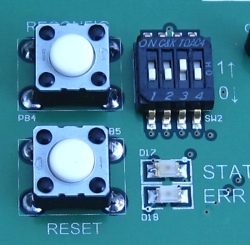
My problem with learning from ambiguous examples... What is the bit ordering of positions 2 to 4, from most to least significant bit? :)
Thanks in advance!
Last edited by David Garcia-Roger (2015-Nov-30 03:22:51)
Offline
#2 2015-Nov-30 02:54:45
- murphpo
- Administrator
- From: Mango Communications
- Registered: 2006-Jul-03
- Posts: 5159
Re: FPGA Config SW2
I'm pretty sure the pins are mapped such that the slot selection value MSB is on the left (i.e. slot_val[2:0] = dip_sw_pos[2:4]). This is based on tracing the pin assignments from the schematics to the CPLD design constraints and HDL. I'm out of the office for a few days, so I can't actually test this to be certain.
Offline
#3 2015-Nov-30 03:08:56
- Christian
- Member
- Registered: 2010-Feb-26
- Posts: 124
Re: FPGA Config SW2
Patrick is right, bit position 2 (towards the RAM) is the MSB.
Offline
#4 2015-Nov-30 03:22:04
- David Garcia-Roger
- Member
- Registered: 2015-Nov-03
- Posts: 10
Re: FPGA Config SW2
Thank you for your quick reply! :)
Offline