WARP v3 User Guide: FPGA Configuration
By default the FPGA is a "blank slate". The FPGA configuration is volatile and must be re-downloaded every time power is cycled. The WARP v3 board provides three FPGA configuration methods: JTAG, SD card and SPI flash.
JTAG
The Xilinx FPGA includes dedicated JTAG pins for in-system configuration and debug. This JTAG interface is routed to a 14-pin connector (J14) on WARP v3. Accessing the JTAG interface requires an external JTAG programming cable. The connector and pinout of J14 complies with the requirements of the Xilinx Platform configuration cables.
The JTAG configuration interface is always enabled and can be used independent of the SD/SPI flash methods described below.
Any JTAG cable supported by Xilinx iMPACT should work. We have tested the JTAG interface with these cables:
- Digilent USB-JTAG Programming Cable
- Digilent HS1 JTAG Programming Cable
- Digilent HS2 JTAG Programming Cable (seemingly incompatible with ISE 13.4; works with ISE 14.3+)
- Xilinx Platform Cable USB II
The JTAG chain connected to J14 requires 2.5v I/O. The Virtex-6 FPGA is the only device on this chain. There is a second JTAG chain on the WARP v3 board which operates at 3.3v. This chain connects to the FMC JTAG pins and the configuration PLD JTAG interface.
SD Card
WARP v3 includes an SD card slot for loading FPGA configurations from removable flash cards. An SD card can contain up to 8 bitstreams, with the active bitstream selected at configuration time via a DIP switch. After loading a bitstream from an SD card, the card can be removed without interrupting operation of the newly-loaded FPGA design. This is very useful for rapidly configuring multiple nodes using a single SD card.
The WARP v3 SD card interface only supports standard SD cards up to 2GB in size. Higher capacity cards using the SDHC or SDXC standards are not supported. The WARP v3 kit ships with a known-good SD card (currently the Transcend TS2GSDC / Amazon link) programmed with a simple test design that displays an incrementing value on the board's hex displays.
Selecting SD Card for Configuration
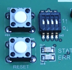
To select the SD card as the configuration source, set position 1 of DIP SW SW2 to 0, as illustrated below.

The WARP v3 configuration PLD implements the following behavior in this mode:
- The PLD acts as an SPI master to access the SD card and a master for the FPGA slave serial configuration mode.
- The SD card will be reset and switched to SPI mode on power up and whenever a new card is inserted.
- A configuration cycle will initiate on power up, when a new SD card is inserted or when you press the RECONFIG push button (PB4).
- During configuration the STAT LED (D17) is driven by the FPGA CCLK signal and will appear to be partially illuminated as the bitstream is loaded. If configuration succeeds the LED will illuminate fully.
- The ERR LED (D18) will illuminate if an error is detected during configuration. The most likely cause of errors is an invalid FPGA configuration bitstream stored in the SPI flash.
Positions 2-4 of the DIP switch select which configuration slot on the SD card should be used for configuration. For example, to select slot 2 on the SD card, set the DIP switch to:

For instructions on writing configuration files to an SD card, see the SD Config Howto.
SPI Flash
The WARP v3 board includes a 128Mb SPI flash device (Numonyx M25P128). This device can be used to configure the FPGA at power-up without an external JTAG cable or SD card. Configuration from SPI flash uses the Virtex-6 Master SPI mode.
Selecting SPI Flash for Configuration
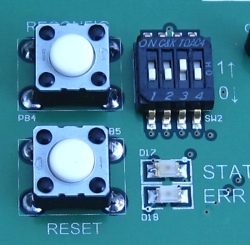
To select the SPI Flash as the configuration source, set position 1 of DIP SW SW2 to 1, as illustrated below.

The WARP v3 configuration PLD implements the following behavior in this mode:
- The FPGA and flash SPI interfaces are tied together with the FPGA acting as SPI master.
- The PLD initiates a Master SPI configuration cycle at power up.
- The RECONFIG push button (PB4) is tied to the FPGA INIT_B signal. Pushing the button initiates an FPGA configuration cycle.
- During configuration the STAT LED (D17) is driven by the FPGA CCLK signal and will appear to be partially illuminated as the bitstream is loaded. If configuration succeeds the LED will illuminate fully.
- The ERR LED (D18) will illuminate if an error is detected during configuration. The most likely cause of errors is an invalid FPGA configuration bitstream stored in the SPI flash.
For instructions on writing a configuration file to the SPI flash, see the SPI Flash Config Howto.
Configuration PLD
The WARP v3 board uses a Xilinx Coolrunner-II PLD to manage the SD card and SPI flash configuration interfaces. This PLD is pre-configured with a standard design which supports both interfaces and implements the behaviors described above. The PLD retains its configuration while powered down. Most users will never need to modify the PLD design.
To load a new PLD configuration use the JTAG interface routed to J17. This JTAG chain also includes the dedicated JTAG pins for the FMC header. Mount a shunt on header J7 to bypass the FMC JTAG interface if no FMC module is mounted or the mounted FMC module does not use JTAG. This JTAG chain uses 3.3v I/O and has been tested with the same programming cables listed above.
The source code for the default PLD design is available in the repository. The SD card configuration mode is based on Arnim Laeuger's spi_boot project from OpenCores. Please see the readme file in the repository for details on licensing and our (thankfully minor) changes to the original spi_boot code.
CPLD - FPGA I/O
In addition to the FPGA configuration pins, there are 11 CPLD pins tied to general purpose FPGA I/O pins. The default CPLD design does not use these signals. They are available for custom designs requiring post-configuration access to the SPI flash or SD card, or any other configuration-related customizations.
The FPGA and CPLD pin assignments are listed below.
| FPGA Pin | CPLD Pin | Net Name | Config Use | FPGA IO After Config |
|---|---|---|---|---|
| R8 | 96 | FPGA_DONE | DONE | No |
| P8 | 95 | FPGA_INIT | INIT_B | No |
| L8 | 94 | FPGA_PROG | PROG_B | No |
| H8 | 76 | FPGA_DIN | SPI MISO | No |
| K8 | 78 | FPGA_CCLK | CCLK | No |
| AA24 | 99 | FPGA_MOSI | SPI MOSI | Yes |
| Y24 | 97 | FPGA_FCS | SPI Chip Select | Yes |
| J25 | 85 | CPLD_GPIO0 | - | Yes |
| N24 | 86 | CPLD_GPIO1 | - | Yes |
| N23 | 87 | CPLD_GPIO2 | - | Yes |
| P24 | 89 | CPLD_GPIO3 | - | Yes |
| R24 | 90 | CPLD_GPIO4 | - | Yes |
| H25 | 82 | CPLD_GPIO5 | - | Yes |
| L24 | 81 | CPLD_GPIO6 | - | Yes |
| H24 | 80 | CPLD_GPIO7 | - | Yes |
| J24 | 79 | CPLD_GPIO8 | - | Yes |
| T24 | 92 | CPLD_GPIO9 | - | Yes |
| T23 | 91 | CPLD_GPIO10 | - | Yes |