| Version 8 (modified by murphpo, 12 years ago) (diff) |
|---|
WARP FPGA Board I/O
USB UART
The FPGA board includes a USB-UART interface, built around the FTDI FT232R transceiver. You can connect this port to a PC via a standard USB cable, and your OS will regonize a new serial port. We have tested this interface in Windows, Linux and OS X. You will need the Virtual COM Port drivers from FTDI.
The transceiver presents a 2-wire (Tx/Rx) UART interface to the FPGA, which can be used with the Xilinx UART transceiver cores.
RS-232 UART
The FPGA board also includes a standard RS-232 serial port. The board's female DB9 port is configured just like a PC, with Tx on pin 3, Rx on pin 2 and GND on pin 5. The rest of the signals are unconnected. You must use a null-modem (i.e. crossover) cable to connect this port directly to a PC.
The LVTTL-RS232 level shifting is handled by a Maxim MAX3319 transceiver.
Digital I/O
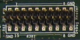
There are 16-bits of unbuffered 3.3v I/O connected directly to FPGA I/O pins, routed to standard male 100mil header. The header has four ground pins in the corner positions. The 16 I/O signals are labeled at the header. Bits 0-7 are in the top row, bits 8-15 in the bottom, both arranged right-to-left.
FPGA Constraints
#FPGA Board v2.2 I/O constraints for Other I/O Devices
#
#16-bits of Digital I/O at 20-pin 0.1" header (component J20)
# 4 corner pins of 20-pin header are ground
# Bit 0 is pin 0, as labeled on the board
Net DIGITAL_IO<0> LOC = L20 | IOSTANDARD = LVTTL;
Net DIGITAL_IO<1> LOC = J21 | IOSTANDARD = LVTTL;
Net DIGITAL_IO<2> LOC = G20 | IOSTANDARD = LVTTL;
Net DIGITAL_IO<3> LOC = J20 | IOSTANDARD = LVTTL;
Net DIGITAL_IO<4> LOC = K21 | IOSTANDARD = LVTTL;
Net DIGITAL_IO<5> LOC = F20 | IOSTANDARD = LVTTL;
Net DIGITAL_IO<6> LOC = H20 | IOSTANDARD = LVTTL;
Net DIGITAL_IO<7> LOC = L21 | IOSTANDARD = LVTTL;
Net DIGITAL_IO<8> LOC = H18 | IOSTANDARD = LVTTL;
Net DIGITAL_IO<9> LOC = H19 | IOSTANDARD = LVTTL;
Net DIGITAL_IO<10> LOC = K19 | IOSTANDARD = LVTTL;
Net DIGITAL_IO<11> LOC = G18 | IOSTANDARD = LVTTL;
Net DIGITAL_IO<12> LOC = F19 | IOSTANDARD = LVTTL;
Net DIGITAL_IO<13> LOC = L19 | IOSTANDARD = LVTTL;
Net DIGITAL_IO<14> LOC = J19 | IOSTANDARD = LVTTL;
Net DIGITAL_IO<15> LOC = F18 | IOSTANDARD = LVTTL;
#
#RS-232 UART Interface (DB9 connector J50)
# Rx is FPGA input, Tx is FPGA output
Net UART_DB9_RX LOC = L24 | IOSTANDARD = LVCMOS25;
Net UART_DB9_TX LOC = K24 | IOSTANDARD = LVCMOS25;
#
#USB-UART Interface (USB connector J58)
# Rx is FPGA input, Tx is FPGA output
Net UART_USB_RX LOC = C23 | IOSTANDARD = LVTTL;
Net UART_USB_TX LOC = AA23 | IOSTANDARD = LVTTL;
#FPGA Board v2.2 I/O constraints for Other I/O Devices # #16-bits of Digital I/O at 20-pin 0.1" header (component J20) # 4 corner pins of 20-pin header are ground # Bit 0 is pin 0, as labeled on the board Net DIGITAL_IO<0> LOC = L20 | IOSTANDARD = LVTTL; Net DIGITAL_IO<1> LOC = J21 | IOSTANDARD = LVTTL; Net DIGITAL_IO<2> LOC = G20 | IOSTANDARD = LVTTL; Net DIGITAL_IO<3> LOC = J20 | IOSTANDARD = LVTTL; Net DIGITAL_IO<4> LOC = K21 | IOSTANDARD = LVTTL; Net DIGITAL_IO<5> LOC = F20 | IOSTANDARD = LVTTL; Net DIGITAL_IO<6> LOC = H20 | IOSTANDARD = LVTTL; Net DIGITAL_IO<7> LOC = L21 | IOSTANDARD = LVTTL; Net DIGITAL_IO<8> LOC = H18 | IOSTANDARD = LVTTL; Net DIGITAL_IO<9> LOC = H19 | IOSTANDARD = LVTTL; Net DIGITAL_IO<10> LOC = K19 | IOSTANDARD = LVTTL; Net DIGITAL_IO<11> LOC = G18 | IOSTANDARD = LVTTL; Net DIGITAL_IO<12> LOC = F19 | IOSTANDARD = LVTTL; Net DIGITAL_IO<13> LOC = L19 | IOSTANDARD = LVTTL; Net DIGITAL_IO<14> LOC = J19 | IOSTANDARD = LVTTL; Net DIGITAL_IO<15> LOC = F18 | IOSTANDARD = LVTTL; # #RS-232 UART Interface (DB9 connector J50) # Rx is FPGA input, Tx is FPGA output Net UART_DB9_RX LOC = L24 | IOSTANDARD = LVCMOS25; Net UART_DB9_TX LOC = K24 | IOSTANDARD = LVCMOS25; # #USB-UART Interface (USB connector J58) # Rx is FPGA input, Tx is FPGA output Net UART_USB_RX LOC = C23 | IOSTANDARD = LVTTL; Net UART_USB_TX LOC = AA23 | IOSTANDARD = LVTTL;
