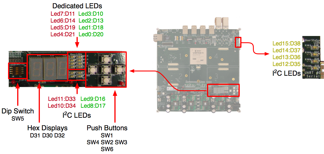
WARP FPGA Board User I/O
The FPGA board includes a variety of interactive I/O devices, referred to as User I/O. These interfaces are intended to aid with observing and debugging custom designs in hardware.
Push Buttons
Five push buttons are connected to dedicated FPGA inputs and are arranged in a cross. They are generally referred as up, down, left, right and center. The buttons are normally open connections with external pull down resistors. Thus, the FPGA will observe logic high when a button is pressed, logic low otherwise.
The switches are debounced by a simple low pass filter on the board, but user applications which are sensitive to accidental or repeated rising edges should further debounce the input digitally.
In our standard EDK designs, the down button is assigned to the PowerPC's soft reset input. When pushed and released, the PowerPC will reset and re-enter the user's main() function. If desired, the choice of the reset button can be changed in an EDK project's hardware specification. Thus four buttons are available for user access.
DIP Switch
The 4-position DIP switch drives four dedicated inputs on the FPGA. Sliding a switch to the left drives the input to logic low; to the right drives the input to logic high.
LEDs
There are 16 LEDs which can be controlled from user designs.
Eight of these are connected to dedicated FPGA I/O pins- four green, four red; their layout shown in the diagram above.
An additional eight LEDs (four yellow, two red and two green) are connected to the FPGA through an I2C I/O expander (MAX7318, component U39). User designs must use an I2C master in the FPGA to control these LEDs.
Hex Displays
There are three 7-segment displays on the FPGA board. All three are connected to the FPGA through I2C I/O expanders (U36 and U39). User designs must use an I2C master in the FPGA to control the displays.
Each display includes eight LED elements- seven forming segments of a numerical digit and one acting as a small decimal point. Each element is controlled individually by separate bits in the I2C I/O expander's register bank.
Your application must handle the mapping of hexadecimal digits to the 7 LED segments.
Custom User I/O Core
We have implemented a custom core which maps all the user I/O available on the board to registers accessible to user designs. Details of the core are available here.
Constraints
#FPGA Board v2.2 I/O constraints for User I/O Devices
#
# 8 LEDs directly controlled using the FPGA I/O pins (D10, D11, D13,
# D14, D18, D19, D20, D21)
NET LED<0> LOC = N24 | IOSTANDARD = LVCMOS25; #RED D11
NET LED<1> LOC = N20 | IOSTANDARD = LVCMOS25; #RED D14
NET LED<2> LOC = L18 | IOSTANDARD = LVCMOS25; #RED D19
NET LED<3> LOC = N18 | IOSTANDARD = LVCMOS25; #RED D21
NET LED<4> LOC = M18 | IOSTANDARD = LVCMOS25; #GREEN D10
NET LED<5> LOC = M25 | IOSTANDARD = LVCMOS25; #GREEN D13
NET LED<6> LOC = N19 | IOSTANDARD = LVCMOS25; #GREEN D18
NET LED<7> LOC = P19 | IOSTANDARD = LVCMOS25; #GREEN D20
#
# 5 pushbuttons arranged a cross orientation.
NET PUSHB_CENTER LOC = L23 | IOSTANDARD = LVCMOS25;
NET PUSHB_DOWN LOC = M21 | IOSTANDARD = LVCMOS25;
NET PUSHB_LEFT LOC = N22 | IOSTANDARD = LVCMOS25;
NET PUSHB_RIGHT LOC = M23 | IOSTANDARD = LVCMOS25;
NET PUSHB_UP LOC = N23 | IOSTANDARD = LVCMOS25;
#
# 4-bit DIP Switch (SW5)
NET DIPSW<0> LOC = M17 | IOSTANDARD = LVCMOS25;
NET DIPSW<1> LOC = R18 | IOSTANDARD = LVCMOS25;
NET DIPSW<2> LOC = P17 | IOSTANDARD = LVCMOS25;
NET DIPSW<3> LOC = M16 | IOSTANDARD = LVCMOS25;
#
# 2 IO Expanders that control the three hex displays (D30, D31, D32) and
# and 8 additional LEDs (D16, D17, D33, D34, D35, D36, D37, D38)
NET HEX_SDA LOC = AL18 | IOSTANDARD = LVCMOS33;
NET HEX_SCL LOC = AK17 | IOSTANDARD = LVCMOS33;
