WARP FPGA Board Memory Resources
ZBT SRAMs
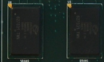
There are two banks of ZBT SRAM on the FPGA board. Each bank is an 18Mbit 36bx512k pipelined zero-bus-turnaround (ZBT) SRAM rated for at least 167MHz operation. Each bank is connected directly to FPGA I/O; no pins are shared between the banks.
The SRAM requires a memory controller in the FPGA. For EDK projects, use the Xilinx PLB External Memory Controller (plb_emc.pdf). This core is included with the EDK. One core is required per SRAM bank. Each should be configured with the following paramters:
 PARAMETER C_NUM_BANKS_MEM = 1
 PARAMETER C_MAX_MEM_WIDTH = 32
 PARAMETER C_INCLUDE_NEGEDGE_IOREGS = 1
 PARAMETER C_INCLUDE_DATAWIDTH_MATCHING_0 = 1
 PARAMETER C_MEM0_WIDTH = 32
 PARAMETER C_SYNCH_MEM_0 = 1
 PARAMETER C_TCEDV_PS_MEM_0 = 0
 PARAMETER C_TWC_PS_MEM_0 = 0
 PARAMETER C_TAVDV_PS_MEM_0 = 0
 PARAMETER C_TWP_PS_MEM_0 = 0
 PARAMETER C_THZCE_PS_MEM_0 = 0
 PARAMETER C_TLZWE_PS_MEM_0 = 0
For projects built using Base System Builder and the WARP FPGA Board XBD, this configuration is automatic.
The SRAM chips used in the current version of the board are Cypress CY7C1307D.
