WARP FPGA Board I/O
10/100 Ethernet
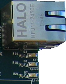
The FPGA board has a 10/100 Ethernet port. This interface uses the Intel LXT972A physical layer Ethernet transceiver. The Ethernet MAC is instantiated in the FPGA. There are three Ethernet status LEDs, described below. These LEDs are only active after the PHY is initialized by a MAC in the FPGA.
The FPGA board's Ethernet interface does not implement auto MDI/MDI-X negotiation.
| Label | Color | Component | Function |
| Activity | Green | D3 | Blinks with network activity |
| Speed | Amber | D6 | Glows for 100Mbit links |
| Link | Green | D7 | Glows with valid PHY link |
Xilinx provides a core which implements the 10/100 Ethernet MAC and attaches to the PLB (plb_emac). An evaluation verison of this core is included with the EDK. The evaluation version functions normally in hardware for a fixed time period (around 7 hours) before disabling itself. The full version can be purchased from Xilinx. Universities can also request a donation of the core.
The pin mapping for the FPGA-PHY interface is listed below. For projects built using Base System Builder and the WARP FPGA Board XBD, this interface is constructed automatically.
| MII Signal | FPGA Pin |
| COL | J26 |
| CRS | D29 |
| MDC | J24 |
| MDINT | G27 |
| MDIO | C23 |
| PAUSE | H27 |
| RESET | J27 |
| RX_CLK | E24 |
| RX_D<0> | C22 |
| RX_D<1> | E21 |
| RX_D<2> | C21 |
| RX_D<3> | D23 |
| RX_DV | F22 |
| RX_ER | F21 |
| TX_CLK | F20 |
| TX_D<0> | D22 |
| TX_D<1> | H23 |
| TX_D<2> | D26 |
| TX_D<3> | G26 |
| TX_EN | H22 |
| TX_ER | H26 |
| TXSLEW0 | H20 |
| TXSLEW1 | J22 |
RS-232 UART
The FPGA board includes a standard RS-232 serial port. The board's female DB9 port is configured just like a PC, with Tx on pin 3, Rx on pin 2 and GND on pin 5. The rest of the signals are unconnected. You must use a null-modem (i.e. crossover) cable to connect this port directly to a PC.
The LVTTL-RS232 level shifting is handled on the FPGA board by a MAX3221 (from Maxim or TI).
The two UART signals are mapped to two FPGA pins:
| Signal | FPGA Pin |
| UART Tx | AA28 |
| UART Rx | AA29 |
Digital I/O
There are 16-bits of unbuffered 3.3v I/O connected directly to FPGA I/O pins, routed to standard male 100mil header. The header has four ground pins in the corner positions. The 16 I/O signals are labeled at the header. Bits 0-7 are in the top row, bits 8-15 in the bottom, both arranged right-to-left. The FPGA pin mapping is below.
| Signal | FPGA Pin |
| Digital I/O[0] | K28 |
| Digital I/O[1] | G30 |
| Digital I/O[2] | H29 |
| Digital I/O[3] | H30 |
| Digital I/O[4] | J28 |
| Digital I/O[5] | F30 |
| Digital I/O[6] | E29 |
| Digital I/O[7] | D30 |
| Digital I/O[8] | K30 |
| Digital I/O[9] | J30 |
| Digital I/O[10] | K29 |
| Digital I/O[11] | J29 |
| Digital I/O[12] | G29 |
| Digital I/O[13] | H28 |
| Digital I/O[14] | F29 |
| Digital I/O[15] | E30 |

