WARP FPGA Board User I/O
Push Buttons
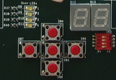
Five push buttons are connected to dedicated FPGA inputs and are arranged in a cross. They are generally referred as up, down, left, right and center. The buttons are normally open connections with external pull down resistors. Thus, the FPGA will observe logic high when a button is depressed, logic low otherwise.
The switches are debounced by a simple low pass filter on the board, but user applications which are sensitive to accidental or repeated rising edges should further debounce the input digitally.
In most FPGA designs, the down button is assigned to the PowerPC's soft reset input. When pushed and released, the PowerPC will reset and re-enter the user's main() function. If desired, the choice of the reset button can be changed in an EDK project's UCF file.
| Button | FPGA Pin |
| Up | AJ22 |
| Down | AM16 |
| Left | AJ15 |
| Right | AG18 |
| Center | AG17 |
DIP Switch
The 4-position DIP switch drives four dedicated inputs on the FPGA. Sliding a switch to the left drives the input to logic low; to the right drives the input to logic high.
| Switch | FPGA Pin |
| 1 (top) | Y27 |
| 2 | Y28 |
| 3 | AA27 |
| 4 (bottom) | Y29 |
LEDs
Four discrete LEDs are connected to four FPGA outputs. A logic high output will cause a LED to glow.
| LED | FPGA Pin |
| 1 (top) | AJ14 |
| 2 | AM13 |
| 3 | AR12 |
| 4 (bottom) | AH13 |
Seven Segment Displays
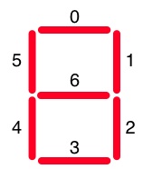
Two 7-segment LED displays are connected to 14 dedicated FPGA outputs, where each segment is driven by an separate FPGA output. The segments are mapped as shown in the image below. The decimal point LEDs on the displays are not used. A logic high causes the corresponding LED segment to illuminate.
Your applicaiton must handle the mapping of hexadecimal digits to the 7 LED segments. Example Verilog and C code is included below which implements this mapping.
| Display | Segment | FPGA Pin |
| Left (D12) | 0 | AJ26 |
| Left (D12) | 1 | AH26 |
| Left (D12) | 2 | AH24 |
| Left (D12) | 3 | AH25 |
| Left (D12) | 4 | AH23 |
| Left (D12) | 5 | AG22 |
| Left (D12) | 6 | AG23 |
| Right (D13) | 0 | AG19 |
| Right (D13) | 1 | AG21 |
| Right (D13) | 2 | AH19 |
| Right (D13) | 3 | AJ19 |
| Right (D13) | 4 | AP12 |
| Right (D13) | 5 | AN13 |
| Right (D13) | 6 | AL15 |
Verilog Hex -> Seven Segment Mapping Example
module sevenSegmentMap
(
    input   [3:0]   fourBitInput,
    output  [6:0]   hexDisplay
);

reg [6:0]   hexDisplay;

always @(fourBitInput[3:0])
    case (fourBitInput[3:0])
        4'b0001 : hexDisplay = ~(7'b1111001);   // 1
        4'b0010 : hexDisplay = ~(7'b0100100);   // 2
        4'b0011 : hexDisplay = ~(7'b0110000);   // 3
        4'b0100 : hexDisplay = ~(7'b0011001);   // 4
        4'b0101 : hexDisplay = ~(7'b0010010);   // 5
        4'b0110 : hexDisplay = ~(7'b0000010);   // 6
        4'b0111 : hexDisplay = ~(7'b1111000);   // 7
        4'b1000 : hexDisplay = ~(7'b0000000);   // 8
        4'b1001 : hexDisplay = ~(7'b0010000);   // 9
        4'b1010 : hexDisplay = ~(7'b0001000);   // A
        4'b1011 : hexDisplay = ~(7'b0000011);   // b
        4'b1100 : hexDisplay = ~(7'b1000110);   // C
        4'b1101 : hexDisplay = ~(7'b0100001);   // d
        4'b1110 : hexDisplay = ~(7'b0000110);   // E
        4'b1111 : hexDisplay = ~(7'b0001110);   // F
        default : hexDisplay = ~(7'b1000000);   // 0
    endcase
endmodule
C Hex -> Seven Segment Mapping Example
unsigned char sevenSegmentMap(unsigned char x)
    switch(x) {
        case(0x0) : return 0x3F;
        case(0x1) : return 0x06;
        case(0x2) : return 0x5B;
        case(0x3) : return 0x4F;
        case(0x4) : return 0x66;
        case(0x5) : return 0x6D;
        case(0x6) : return 0x7D;
        case(0x7) : return 0x07;
        case(0x8) : return 0x7F;
        case(0x9) : return 0x6F;

        case(0xA) : return 0x77;
        case(0xB) : return 0x7C;
        case(0xC) : return 0x39;
        case(0xD) : return 0x5E;
        case(0xE) : return 0x79;
        case(0xF) : return 0x71;
        default   : return 0x00;
    }
}

