WARP FPGA Board Power Supplies
Required External Supply
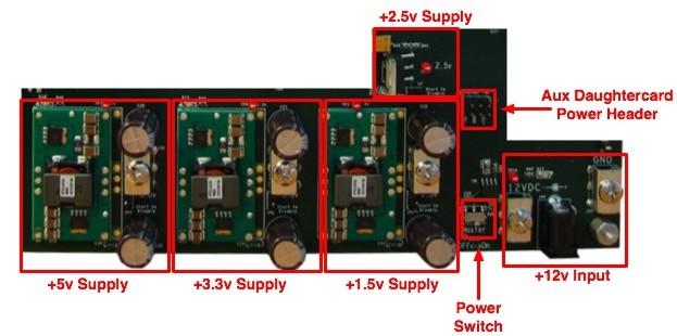
The WARP FPGA board operates from a single external 12v supply. This supply is generally connected to the board's coaxial power connector. This connector requires a mating female connector with an inner diameter of 2.1mm, outer diameter of 5.5mm, positive tip and grounded shell. We use the 30W AC-DC regulator from Astrodyne (SPU30-105).
FPGA Power Supplies
The Virtex-II Pro FPGA has a number of different power inputs. The table below summarizes the power supplies on the WARP FPGA board.
| Supply | Voltage | Description |
| VCC_INT | 1.5v | FPGA core logic |
| VCC_AUX | 2.5v | FPGA clock resources |
| VCC_O | 3.3v | FPGA I/O banks |
| AVCCAUXRX | 2.5v | MGT Rx logic |
| AVCCAUXTX | 2.5v | MGT Tx logic |
| VTTX | 2.5v | MGT Tx termination |
| VTRX | 2.5v or 1.8v | MGT Rx termination |
The WARP FPGA board uses switching power supplies for the 1.5 and 3.3v supplies. Both supplies are Texas Instruments' PTH12020W 18A DC-DC power modules.
The 2.5v VCC_AUX supply is a LT1963A linear regulator from Linear Technology.
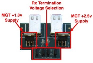
The MGT supplies are all driven by linear supplies in order to minimize noise in the MGT circuitry. Two LT1963A linear regulators are used, one configured for 1.8v output, the other for 2.5v. The receive termination voltage (VTRX) for four MGTs can be configured for either 1.8v or 2.5v. Four 3-pin jumpers are used to select VTRX for MGTs 3, 4, 5 and 6. A 2-pin shunt should be mounted on each 3-pin jumper, shorting either the bottom two or top two pins of each jumper. Shorting the bottom two pins selects 2.5v; shorting the top two selects 1.8v. These jumpers should generally be configured for 2.5v.
Daughtercard Power Supplies
The four daughtercard slots on the WARP FPGA board are supplied with 5v by a dedicated 18A switching regulator. A second power plane is also connected to the daughtercard slots and can be driven by an off-board supply via a dedicated 6-pin header on the FPGA board. This header, component J35, is usually not mounted.
Monitoring Voltage Levels
Every power and ground plane on the FPGA board includes a test point which can be used to monitor the plane's voltage. The 7 test points on each voltage plane are red and are labeled on the board. The 3 ground test points (1 for MGT ground, 2 for digital ground) are black.
Every power plane except the 1.5v VCC_INT supply also includes a red LED which glows when power is applied. These LEDs should always be illuminated when the FPGA board is powered on. If any of these LEDs is not glowing, immediately power off the board to avoid damaging components.
Bypassing Power Supplies
The WARP FPGA board does not contain any built-in current measurement capabilities. In order to measure current consumption, the power plane of interest must be driven by an external, off-board supply whose current can be measured. When an external supply is used, the on-board regulator for a given plane must be disabled to avoid a drive fight between the on-board and off-board supplies. Four of the FPGA board's supplies (5v, 3.3v, 2.5v and 1.5v) can be individually disabled. To disable these regulators, simply mount a shunt on the jumper adjascent to the regulator; see the table below for the specific reference designators for each jumper.
High-current screw terminals are connected to the primary power planes: GND, 12v, 5v, 3.3v and 1.5v and can be used to connect external supplies. See the image below to identify the screw terminals.
The MGT power planes (2.5v, 1,8v) cannot be disabled and should never be driven externally.
| Plane | Regulator | Disable Jumper | Screw Terminal | Test Point |
| 5v | U9/U10 | J40 | J38 | TP7 |
| 3.3v | U11/U12 | J41 | J37 | TP6 |
| 2.5v | U7 | J34 | - | TP4 |
| 1.5v | U13/U14 | J42 | J36 | TP5 |
| GND | - | - | J39 | TP8 & TP9 |


