| Version 7 (modified by murphpo, 17 years ago) (diff) |
|---|
WARP FPGA Board I/O
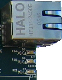
10/100 Ethernet
Intel LXT972A physical layer Ethernet transceiver
Three status LEDs. LEDs only work after the PHY is initialized by a MAC in the FPGA.
| Label | Color | Component | Function |
| Activity | Green | D3 | Blinks with network activity |
| Speed | Amber | D6 | Glows for 100Mbit links |
| Link | Green | D7 | Glows with valid PHY link |
RS-232 UART
FPGA board configured just like a PC- male DB9 connector, Tx on 3, Rx on 2, GND on 5. Null-modem (crossover) female-female cable required to connect to PC's serial port.
Digital I/O
There are 16-bits of unbuffered 3.3v I/O connected directly to FPGA I/O pins, routed to standard male 100mil header. The header has four ground pins in the corner positions. The 16 I/O signals are labeled at the header. Bits 0-7 are in the top row, bits 8-15 in the bottom, both arranged right-to-left. The FPGA pin mapping is below.
| Signal | FPGA Pin |
| Digital I/O[0] | K28 |
| Digital I/O[1] | G30 |
| Digital I/O[2] | H29 |
| Digital I/O[3] | H30 |
| Digital I/O[4] | J28 |
| Digital I/O[5] | F30 |
| Digital I/O[6] | E29 |
| Digital I/O[7] | D30 |
| Digital I/O[8] | K30 |
| Digital I/O[9] | J30 |
| Digital I/O[10] | K29 |
| Digital I/O[11] | J29 |
| Digital I/O[12] | G29 |
| Digital I/O[13] | H28 |
| Digital I/O[14] | F29 |
| Digital I/O[15] | E30 |

